A team at Stanford University working on single sheets of graphene found that this curious material, only 1 atom thick, is 100 times more chemically reactive than double or triple sheets. The scientists note, in a paper published in ACS Nano , that understanding graphenes chemical reactivity is key to putting the unique material to work.
Graphene is a chicken-wire-like structure of carbon atoms that is highly conductive, super light, and super strong. It holds promise for applications in computing, solar energy, and chemical sensing. Convinced there is more to come, materials scientists are still teasing out graphene's remarkable properties and potential uses.

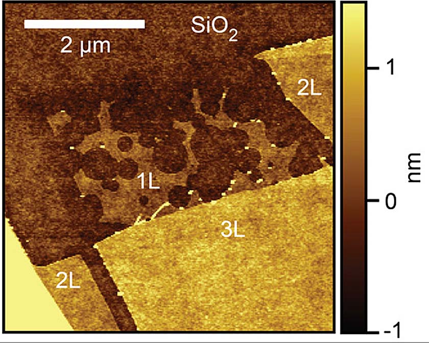
Single layers of the novel material graphene (1L) are etched and pitted by hydrogen plasma, while double and triple layers (2L and 3L) are unscathed.
When they examined the graphene, they found something surprising: The single layers of graphene were riddled with etch pits, like Swiss cheese. Thicker layers, even 1 atom thicker, were hardly pitted at all.
The pits are caused by carbon atoms in graphene reacting with hydrogen atoms, presumably creating methane molecules that lift up and away out of the graphene sheet. The sheets rest on a silicon oxide substrate, which is a participant in the etching reaction. Multilayer sheets are more protected from the substrate's effect.
The researchers also noticed that monolayer etch pits were circular, while the few etch pits found in thicker layers were hexagonal. Why the difference? “The short answer is, we don't really know,” Neumann said, but he speculates that the substrate's participation in the etch reaction could be the cause.
Graphene was famously discovered in 2004 by scientists in England who used adhesive tape to peel single layers of graphene off larger graphite flakes. Diankov and Neumann used the same technique to prepare graphene samples for their experiments. The “exfoliated” graphene sheets can be seen with a simple optical microscope. Layered on the gray silicon substrate, the graphene looks like overlapping dark paint strokes.
Advertisement
Learn more about Electronic Products Magazine


