2- and 3-D bent nanowires are grown with built-in diodes, FETs
Scientists at Harvard University led by Bozhi Tian and Charles M. Lieber have determined how to design and grow nanowires with kinks, transforming them into zigzagging two- and three-dimensional structures with advanced functions. Theses bent monolithic semiconductor nanowires can be made with dopant-modulated structures in which specific device functions, including p–n diodes and field-effect transistors, can be precisely localized at the kinked junctions.
Scientists have been trying to control and modulate the composition, doping, crystal structure, and morphology of semiconductor nanowires during the synthesis process for several years. However, despite advances in nanowire synthesis, design and growth of hierarchical nanostructures has been limited.
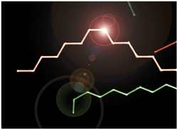
This false-color scanning electron microscope image shows zigzag nanowires in which straight sections are separated by triangular joints. Specific device functions are precisely localized at the joints. (Image courtesy Bozhi Tian/Lieber Group.)
The researchers’ so-called nanotectonic approach provides iterative control over the nucleation and growth of nanowires, allowing them to create zigzagged nanowires in which the straight sections are separated by triangular 120 joints. The lengths of the straight sections can be controlled and the growth direction remains coherent along the nanowire.
To control introduction of fixed joints, referred to as stereocenters, the researchers halted growth of the nanostructures for 15 s by removing key gaseous reactants, then replaced these reactants after joints had been introduced. The distance between kinks is precisely controlled, and the approach has resulted in a 40% yield of bent nanowires, which can then be purified to achieve higher yields. Tian, notes that “we demonstrated the generality of our approach through synthesis of 2-D silicon, germanium, and cadmium sulfide nanowire structures.”
Lieber points out that the nanostructures make possible the integration active devices in nanoelectronic and photonic circuits, thus opening up “totally new approaches for extra- and intracellular biological sensors. This latter area is one where we already have exciting new results, and one we believe can change the way much electrical recording in biology and medicine is carried out.”
The work was funded by the National Institutes of Health, the McKnight Foundation, the MITRE Corp., and the National Science Foundation. For further information, contact Harvard via the Web page http://harvardscience.harvard.edu/contact.
Richard Comerford
Advertisement
Learn more about Harvard Univerity


