A team of researchers at the National University of Singapore (NUS) has figured out a way of (significantly) improving upon the photoluminescent efficiency of tungsten diselenid.
Should the discovery prove scalable, it will likely have a major impact on a variety of optoelectronics and photonics-based applications, including quantum dots, LEDs, photovoltaics, and more.
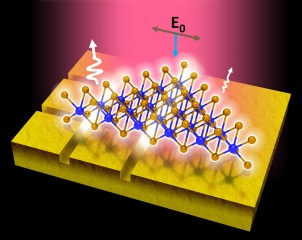
These technologies already use tungsten diselenid for its ability to convert light to electricity (and vice versa), but that’s all it’s been used for. You see, the material’s incredible thinness – while ideal for design purposes – actually hampers its ability to absorb photons and its photoluminescence.
To overcome this limitation, the NUS team used plasmonic nanostructures, as they’ve proven capable of exploiting oscillations in the density of electrons generate whenever photons hit a metal surface; so much so that the improved brightness of tungsten diselenid’s photoluminescence was measured to be in the range of 20,000 times over.
Previous attempts to improve the photoluminescence of tungsten diselenid managed to make it shine (just) 1,000 times as bright as it does in its natural state.
“This is the first work to demonstrate the use of gold plasmonic nanostructures to improve the photoluminescence of tungsten diselenide,” said Wang Zhuo, one of the NUS researchers and first author of the paper, in a press release. “We have managed to achieve an unprecedented enhancement of the light absorption and emission efficiency of this nanomaterial.”
Specifically, the team suspended flakes of tungsten diselenid over sub-20-nanometer-wide trenches in a gold substrate. The reason why this design results in such a huge increase is due to the enhanced absorption of the photons emitted by the pump laser; that is, the absorption boost is due to the plasmons that are confined in the trenches.
“The key to this work is the design of the gold plasmonic nanoarray templates,” said Andrew Wee, a professor at NUS, in the press release. “In our system, the resonances can be tuned to be matched with the pump laser wavelength by varying the pitch of the structures. This is critical for plasmon coupling with light to achieve optimal field confinement.”
Looking ahead, the team will next examine how effective the gold plasmons are when it comes to enhancing electroluminescence of transition metal dichalcogenides. They also plan to extend the investigation into a range of 2D transition metal dichalcogenides with multiple band gaps. The expectation, in this regard, is that each one will employ different interaction mechanisms.
To learn more, download the paper — Giant photoluminescence enhancement in tungsten-diselenide–gold plasmonic hybrid structures.
Via the National University of Singapore
Advertisement
Learn more about Electronic Products Magazine


