Die- and package-on-package stacking technologies help preserve precious PCB space in portable/handlheld devices
BY RICHARD CRISP
Tessera
San Jose, CA
http://www.tessera.com
Consumer handheld and portable electronic devices are now one of the major consumers of advanced semiconductors. For example, shipments of cellular handsets for 2007 were expected to top 1.2 billion units.
Today’s typical cellular handset now contains microwave RF devices, one or more highly integrated digital baseband processors, one or two high-resolution digital camera modules, high-density memory including nonvolatile storage, sophisticated power management, and a GPS receiver—all in a very small form factor. Integration of this density would not be possible without the use of chip-scale packaging (CSP).
CSP alone, however, is not sufficient to support all the miniaturization requirements for this type of product. Three-dimensional (3-D) packaging extends the capabilities of CSP by die-stacking and package-on-package (PoP) stacking. These 3-D packaging technologies further densify the electronics and preserve precious PCB space by exploiting 3-D interconnects for circuit routing while offering several manufacturing advantages for the OEM.
PCB complexity
As an illustration of how 3-D routing can simplify a PCB design, consider the case of dissimilar memory chips such as NAND flash, NOR flash, and DRAM being stacked together. Each of these chips connects to a data bus that connects to a processor.
The stack of the three dissimilar memory chips occupies a footprint slightly larger than a single chip. However, stacking these devices vertically saves the footprint space of the two other chips plus the routing area. Since most of the signals are contained within the memory/processor stack, fewer need to be routed on the PCB, which saves area, complexity, and PCB routing layers, thereby reducing cost.
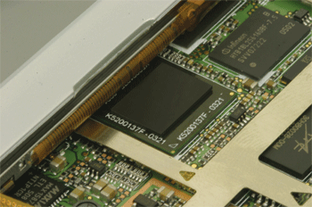
Fig. 1. HP’s IPAQ pocket PC features memory stacked on top of the processor using a stackable BGA package.
One example is seen in the HP IPAQ pocket PC, where memory is stacked atop the processor using a stackable BGA package (see Fig. 1 ). Another example is the Apple iPhone, which has a mobile DRAM stacked on top of a processor, again using stackable BGA technology.
A platform approach
Area savings aren’t all the advantages of PoP stacking of components. Many handset designs can be created from a basic platform approach similar to a PC: PCB, chipset, and various peripheral components combine to make a phone with a certain set of features.
The chipsets are often designed to accommodate package stacking and this can offer an easy way to make derivative products from a base design. In one commonly used method, the amount of memory can be varied to differentiate one product from another.
When the memory is placed in PoP stacks, it is a simple matter to substitute one or more memory components in the stack for different components containing a different amount of memory or perhaps a different set of features. In this way, a family of products can be quickly and easily implemented.
Designers just need to change the number and density of memory components in the common-stack footprint to differentiate the various product offerings in the family. As an example, Apple recently introduced the iPhone in both 4- and 8-Gbit versions — an assembly-time build-option on the part of Apple.
In this case, the NAND flash TSOP packages each contained stacks of four NAND flash die, but the packages were also stacked on top of each other, enabling a 4- or 8-Gbit configuration selection simply by selecting the appropriate stack of memory. This selection can literally be made as a last decision before the handset is assembled, permitting the manufacturer to react quickly to changing market conditions that often occur in the component or handset markets.
PoP stacked ICs
Using die stacking exclusively requires any stacking variants to be made at the time the die are assembled into the packages rather than at the time of the final assembly of the end product. This increases the amount of time needed to make a differentiated product and also may increase the component inventory for the component and handset manufacturer.
Using PoP stacking, the process is simplified and streamlined. A different set of components is stacked together in packaged form. This can be done by the handset manufacturer and very late in the process, if desired.
This enables derivative products to be deployed in a simple and cost-effective manner using a small stock of standardized components. It can also be done very quickly and efficiently, with minimal impact on work-in-process inventory. Alternatively, assembly contractors can supply completed stack subassemblies ready for final assembly.
The advantages for the end-product manufacturer are multifold: a quick and easy process to develop derivative products by changing the elements in the PoP stacks, an efficient use of inventory (mix and match standard components to make derivative products), and reduced time to market for introducing product variants to take advantage of changing market conditions quickly and efficiently. For PCB assembly, the use of PoP stacks reduces the number of piece parts needed to be picked and placed, further reducing cost.
Manufacturing infrastructure
Irrespective of the advantages to the end-product OEM, the advantages of PoP stacking would not be attainable without the supporting infrastructure from component vendors, assembly equipment suppliers and package vendors all working together to develop standards for use. As of mid-2007, 15 major logic IDMs, eight major memory suppliers, six different assembly equipment vendors, and five EMS/CM assembly houses have all agreed to support PoP stacking.
Further footprint reductions
Different methods have been developed for PoP stacking, with most relying on BGA technology. Some cases require a higher-density interconnection than can be supported by BGA technology.
Solder-ball diameters need to remain reasonably large to provide mechanical reliability, but high routing density requires smaller sphere diameters. The industry is looking at new methods to extend interconnection densities without incurring significant increases in cost and assembly time.
One new approach from Tessera, the µPILR platform, offers significantly reduced lead pitch over conventional BGA technology through the use of a solid copper contact technology.
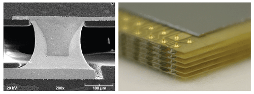
Fig. 2. Tessera’s µPILR platform features pitches as small as 150 µm.
The nickel/gold-plated copper contacts can be placed on a pitch as small as 150 µm to support advanced PoP stacking requirements including large area arrays or tall stacks of memory (see Fig. 2 ). This type of technology offers several advantages, including thin stacks, rework, and light weight in addition to low cost, as well as component test permitting the use of contactor-less test sockets. Not only is the test-socket cost reduced and reliability at test improved, the electrical performance of the device under test more closely approximates the end use when the socket’s electrical contactors are eliminated. ■
For more on 3-D packaging in cellular handsets, visit http://electronicproducts-com-develop.go-vip.net/packaging.asp.
Advertisement
Learn more about Tessera


