By BRIAN NARVESON and ERNIE PARKER, Co-chairman Pkg Committee
PSMA Oranization
www.psma.com
More power in the same footprint is the constant request of the power industry’s customers. This challenge has hit a fever pitch as digital semiconductor packaging technology has increased performance with wafer stacking through the use of wafer thinning and through-silicon-via (TSV) technology. In addition the introduction of 2.5D and 3D integration, has facilitated heterogeneous (“More than Moore”) integration. Use of this technology is increasing as conventional die shrinking has hit a “cost barrier” brought about when advanced deep-submicron semiconductor technology could no longer reduce cost with the addition of more functions to the semiconductor die. 3D packaging and integration allowed the power requirements of the digital load to increase two to five times, within the same footprint, in a single generation. Now the power industry is tasked with finding new ways to package power sources that will meet this demand, but without increasing footprint.
In parallel, power semiconductor technology is facing a “construction barrier” that prevents the realization of the significant benefits new technology can offer in terms of increased power efficiency and higher power density. These new technologies, including gallium-nitride (GaN), silicon-carbide (SiC), and gallium-arsenic (GaAs) power semiconductor devices, all require operation in a package that is free of bond wires and that minimizes parasitic interconnect elements. Both of these challenges can be addressed with power packaging using embedded substrate technologies.
To investigate this technology the Power Sources Manufacturing Association (PSMA) commissioned a report “Current Developments in 3D Packaging with Focus on Embedded Substrate Technologies”. The 340 page report, prepared under contract by LTEC Corporation is based on the Packaging Committee’s extensive research of over 750 articles and papers, and by conducting 30 industry expert interviews.
For the purpose of this article the following definitions apply: Embedded substrate technology is defined as the inclusion of at least one active or passive electrical component within the top and bottom conductive layers of a substrate, with a substrate defined as a planar structure having multiple conductive and insulating layers. Fig. 1 provides an example of this technology based on Shinko Electric Industries Co.’s (Shinko) Molded Core embedded Package (MCEP) process.
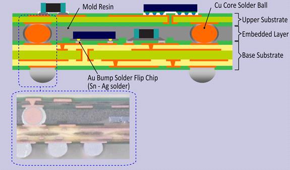
Fig. 1: Example of embedded substrate technology (Shinko MCEP).
As part of the project 30 companies were surveyed to determine why they were actively producing or developing power sources utilizing embedded technology and at what power level they were considering for this technology. The survey found the overriding reasons for using the technology was to reduce size (increase power density) and improve performance. It also found development activity at power levels up to and exceeding 1,000 Watts.
The core technology required for embedding is a PCB or Inorganic Substrate. AT&S is the leader in shipping power sources with embedded substrates. The AT&S Embedded Component Packaging (ECP) process is depicted in Fig. 2. AT&S manufactures on 18 x 24-in. panels, has shipped over 100-million units, and claims >99% yield. Their process is used by Texas Instruments and GaN Systems for embedding of their semi-conductor devices.
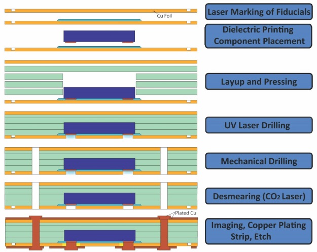
Fig. 2 AT&S Embedded Component Packaging (ECP) Process Flow
An overview of several of the processes available for making embedded substrate power assemblies are listed below. Details and additional processes can be found in the report.
TDK-EPC Corporation has developed its own process named Semiconductor Embedded in Substrate (SESUB). Their embedded process is suitable for high density power supply modules or subsystems, either as substrates or interposers, with or without over-molding. A benefit of SESUB is the ability to have complete metal shielding of the package, an attractive feature for EMI reduction.
General Electric has been a pioneer in recognizing the benefits of component embedding and in technology development, beginning with technology for chip embedding in the 1990’s. GE’s Power Overlay Technology (POL), is backed by a strong portfolio of over 300 patents. GE is actively engaged in licensing its technology.
Infineon developed a variant of the AT&S process that is similar to TDK-EPC’s SESUB and have used that in their Dr. Blade product family
Schweizer AG’s P2 -PAK process was an early entrant to embedding developed as an alternative to expensive direct-bond-copper (DBC) for high current inverters, converters, industrial motor drives, and automotive applications.
Shinko’s MCEP process shown in Fig. 1 is advertised as a low cost solution. Additional processes from Fujikara, Wurth Electronik, and Semikron are covered in the technology report.
The second key technology for embedding is the availability of components. There are two classes of embedded components. First, there is the discrete device, termed the “inserted” component. In this case, the surface mount passive device, R L or C, is manufactured prior to assembly in the printed circuit board. Usually these are mounted in laser machined cavities within the printed circuit board. Semiconductor devices are also inserted and connected to the substrate using a variety technics.
Secondly there is the “formed” component that is manufactured as element(s) within the printed circuit board. All three types of passives (resistors, capacitors and inductors) can be formed in an imbedded substrate. Fig. 3 illustrates the various types of embedded components and shows how they can be implemented in a PCB substrate.
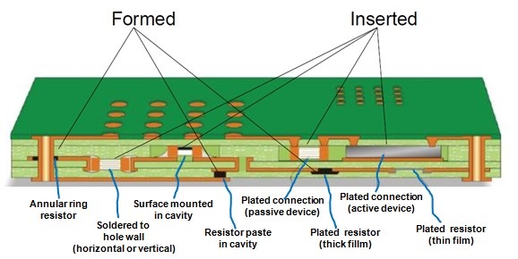
Fig. 3 Example of an embedded assembly.
The ability to execute an embedded power design is very dependent on the availability of inserted passive components, optimized for PCB embedding purposes. The report devotes individual chapters to resistors, capacitors and inductors. Availability of power devices is still somewhat limited in terms of form factor and terminal metallurgy but the number of sources is expanding rapidly. The report also provides lists of vendors with production parts available now.
Successful transition to full volume manufacturing depends on advances in supply chain and technology for compatible passive component technologies. While this article focused on embedded substrate component technology, the 3D Embedded Substrate Technology report also covers the current state of the art as well as challenges and constraints in semiconductors, passive components, high temperature die-attach, interposers, thermal management, packaging technologies, additive manufacturing and laser fabrication, all of which will play a role in the success and timing of a transition to 3D power packaging.
Another sign of the maturing of embedded substrate technology is the number of standards completed and being written. IPC has published embedded standards for, resistors (IPC-4811), capacitors (IPC-4821), printed circuit boards design (IPC-2316) and materials (IPC-4101) plus one being written on design and assembly processes (IPC-7092). Substrates, components and manufacturing processes are available and being developed to meet these standards. There is more elaboration on standards in the report.
In summary, there has been substantial progress and excellent opportunities lie ahead for the power electronics and semiconductor industries and the entire manufacturing ecosystem to embrace PCB embedding and 3D packaging technologies for power electronic applications. The intersection of these technologies with the emerging wide-bandgap power semiconductor technology creates truly exciting possibilities. These technologies, combined with wide-bandgap semiconductor devices will literally re-vitalize the entire power electronic infrastructure for the twenty-first century.
The PSMA reports on 3D packaging are provided free of charge to PSMA members. Others interested in the reports may order a copy from PSMA at http://www.psma.comc/publications .
Advertisement


