By SIMON FRIED
Co-Founder and Chief Marketing Officer
Nano Dimension
www.nano-di.com
Three-dimensional printing of printed circuit boards (PCBs) allows designers and engineers to test out ideas before committing to expensive tooling and manufacturing. Because they rapidly and affordably generate testable concepts, 3D-printed prototypes help users optimize designs and avoid design flaws during the early stages. The result eliminates costly rework and provides significant value in the product-development process.
For companies with design teams, 3D printing is rapidly turning into a must-have technology. It optimizes efficiency, minimizes IP security risks and helps users meet product quality goals. This often makes the difference, enabling high-quality, on-time and innovative product development that improves time-to-market and time-to-revenues.
Bringing PCB prototyping up to speed
Recent advances in 3D printers, along with the development of conductive inks, are providing tremendous value to electronics designers seeking solutions to tackle the major challenges of new product design at the lowest cost and within the shortest time frame.
In the electronics industry, a widely recognized concern among designers and engineers is the design, testing and integration of multilayer PCB prototypes in an electronics product. The more intricate the design, the more expensive the setup costs as well as the overall risk and expense of the prototype. 3D printing a PCB makes manufacturing a complex multilayer PCB much easier by cutting out several steps. Normal PCB manufacturing technology requires blind and open vias to be drilled and plated; the 3D-printing process simply prints them.
The complexity of PCB design also often means that production is outsourced to an overseas facility that turns the PCB design into a prototype and sends it back, usually after several days or weeks have passed. If the prototype reveals any flaws, further iterations can add additional days or weeks to redesign. In highly competitive markets like consumer electronics, this time lag can be very costly. PCB development presents a risk to on-time product development and 3D printing can minimize this risk.
3D inkjet multilayer PCB printing offers the kind of flexibility and responsiveness required in today’s competitive world and eliminates many of the drawbacks associated with outside PCB printing facilities. It lets the designer rapidly build functional prototypes in-house, thus helping to identify product defects in the initial stages of design. Using conductive and dielectric inks, it is possible to produce and test professional multilayer prototype PCBs with interconnections and through-holes in hours – including even the most complex designs (Fig. 1 ).
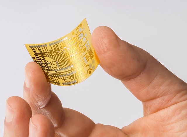
Fig. 1: 3D PCB printing can let designers go beyond traditional PCB design to verify more complex technologies that open up new applications. (Photo: Yoram Reshef)
Apart from rapid prototyping, PCB prototypes created with a 3D printer allow users to create models that would normally be very difficult or even impossible to produce, or that would be time-intensive using current standard subtractive manufacturing processes.
Beyond traditional PCB design
3D PCB printing will also open up many new material choices. If the design has certain mechanical requirements – extra-rigid, flexible or even transparent – 3D printing technology will ultimately offer a material for the job. The printer can import Gerber files, so setting it up for printing is easy. Similarly, there are few limits on how the board is designed. For instance, there are no limits on the number of layers beyond the mechanical height of the z-axis of the printer. Moreover, designers can print circuit geometries using 3D printing that are not possible to manufacture any other way.
Apart from functionality and early testing, 3D printing reduces the risk of sending out intellectual property (IP) in the form of PCB designs. No matter how trusted the partner, no matter how secure the outside facility, the risk of corporate sabotage or design theft increases as soon as your designs leave your facility.
As 3D printers become more available and technology continues to advance, more and more electronics companies will be using them for product development and manufacturing. Planned as the first commercially available 3D PCB printer, DragonFly 2020 3D Printer from Nano Dimension (Fig. 2 ) is a highly accurate and versatile inkjet deposition system for printing multilayer circuit boards. The innovative hardware, dedicated nano-inks — including proprietary highly conductive silver nano-inks — and novel software bring new possibilities to a wide range of R&D, prototyping, and custom-manufacturing projects.

Fig. 2: The DragonFly 2020 3D Printer features a printing size of ca. 20 x 20 cm. The printer prints traces ≈90 µm, ≈150 µm vias, and a minimum layer thickness of 2 to3 µm. (Photo: Yoram Reshef)
Advertisement
Learn more about Nano Dimension


