A design strategy for
system-on-a-chip testing
ensure more testable designs
BY BEN BENNETTS
LogicVision
San Jose, CA
A system-on-a-chip (SOC) is loosely defined to be a device that incorporates
many complex modules within the bounds of a single chip. Module examples
include embedded cores, multiple memories, application-specific user logic,
and possibly analog circuitry.
By their nature, SOCs are often quite large, containing one million
transistors or more and measuring 20 x 20 mm or larger. Consequently, they
cannot be considered as single entities for the purpose of test. SOCs require
specific test algorithms for individual modules, making them too complex
for any traditional automatic-test-program- generation process.
The complexity of SOCs points to a “divide and conquer” approach
to test, but two major problems arise from such a strategy. First, it is
difficult to isolate and access the boundary of a module from the chip's
I/O pins in order to test the modules themselves (intramodule test) or
the interconnects between the modules (intermodule test). Second, it becomes
difficult to automate the process of assembling the set of intermodule
and intramodule tests for the complete chip.
There is an approach–called boundary scan–that has worked at the board
level that may be applied to the design modules of an SOC. However, because
the modules of an SOC are not pretested before assembly, the designer must
ensure that all modules are individually testable. To achieve high-quality
testing, modules must be isolated from one another and accessible from
the SOC's boundary.
Chip designers can address the problems of access and isolation by combining
two design-for-test approaches. Built-in self-test (BIST) technology can
be applied to test individual modules, while peripheral-access (PA) techniques
can be used to solve isolation, access, and intermodule problems. Together,
the BIST and PA methods provide a natural automated solution for testing
SOCs.
Isolation and access
There are a variety of ways to isolate and access any particular embedded
module or core:
1. Accessing a module directly via the I/O pins of the device.
2. Accessing indirectly using multiplexer and demultiplexer switches.
3. Bypassing other modules using PA paths based on existing peripheral registers
or add-on peripheral registers.
4. Using existing feedthrough structures, such as scan registers, inside other
modules: serial in/parallel out on the input side and parallel in/serial out on the output side.
5. Exploiting natural transparency modes to pass data through a module without
change. For example, in an ALU module, A + B = A if B = 0.
The designer needs to select a combination of one or more of these techniques
to ensure adequate controllability and observability on each module in
the design (seeFig. 1 andtable ). In reality, an SOC designer
will try to build on the design's natural access properties (direct, multiplexing/demultiplexing,
feedthrough, and transparency).
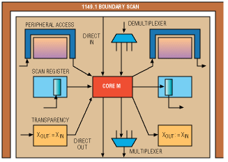
Fig. 1. The system-on-a-chip designer can combine isolation and
access techniques to ensure adequate controllability and observability of each module.
Comparison of peripheral-access techniques
| TECHNIQUE | STRENGTHS | WEAKNESSES |
| Direct access | / Simple interface | / Expensive in I/O pins / Not suitable for interconnect test / Can lead to routing congestion |
| Multiplexing/ demultiplexing |
/ Easy to automate | / Limited to one-at-a-time (serial) test / Not suitable for interconnect test |
| Peripheral access | / OK for serial and parallel test / OK for interconnect test |
/ May require extra silicon (but see text) |
| Feed through | / Makes use of existing design-for-test structures |
/ May only provide limited access to other modules |
| Natural transparency | / Makes use of mission-mode behavior |
/ May not exist in many modules / Difficult to identify and enhance automatically |
However, access for test purposes is often inadequate and the circuit
must be modified. Under this circumstance, an automated analysis and enhancement
system is preferred to a manual approach. PA techniques lend themselves
to automation and also provide a solution to both intermodule and intramodule
test requirements.
Peripheral-access techniques
There are essentially two forms of peripheral access–augmented and
separate. Often, complex modules or predesigned cores come with input and
output registers on data lines. Such structures can be augmented to include
register elements on all other signal lines in and out of the module, thus
forming an augmented PA structure.
Alternatively, where such structures do not already exist, a separate
PA structure can be added to each module during its insertion in the design.
Clearly, there should be no impact on performance, and timing-sensitive
signals can be omitted from the structure if the reduction in testability
is acceptable (seeFig. 2 ).
Once established, PA structures can either be accessed independently
(parallel access) or dependently (serial access). In the latter case, modules
are linked together to form a global boundary-scan-like structure.
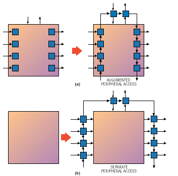
Fig. 2. Peripheral-access structures can be designed by augmenting
modules
or cores that already include input and output registers for data (a) or–where
such registers do not exist–by creating a separate structure (b).
For deeply embedded modules, parallel access is more demanding of I/O
pins but allows parallel testing of each module, whereas serial access
has the reverse of these properties. Both setups lend themselves to module
interconnect test using traditional boundary-scan algorithms such as enhanced
binary count (the Wagner algorithm).
Module/core test issues
PA techniques can be compared to the IEEE 1149.1 boundary-scan techniques
used at the board level but with one important distinction. Unlike devices
mounted onto a bare board, SOC modules have not been pretested before assembly
into the full device.
This means that designers must not only ensure access to the modules,
but also complete testability. It must be possible to generate an adequate
set of test patterns and apply them to the modules.
Traditionally, embedded modules would be tested with a pattern set applied
through the I/O pins by external automatic test equipment (ATE). However,
the need for very high fault coverage–including at-speed tests to catch
dynamic faults–suggests that a better solution is to build the tests into
the module using BIST technology. A simplified “runBIST” protocol
can be used to control the application of the tests and analysis of the
pass/fail result.
A built-in self-test solution, combined with PA techniques, also solves
other SOC problems, namely:
/ Even serial PA can be used to test modules
in parallel.
/ The embedded BIST structures can be re-used
throughout the life cycle of the product (including system and field service)
and con- trolled by much cheaper exter- nal ATE.
/ For cores, the core provider can protect
its intellectual property without compromising testability.
Commercially available tools allow an SOC designer to incorporate self-test
into a complex module or soft core that has been described at the register-transfer
level with a hardware description language such as VHDL or Verilog. To
be of value, such tools should accommodate a variety of internal blocks
including SRAM, DRAM, ROM, and scan-based user logic.
The tools should also be able to insert boundary scan to the IEEE 1149.1
standard. An example is LogicVision's icBIST product. In addition to being
able to add the self-test and boundary-scan hardware, this software is
capable of linking the 1149.1 TAP controller to internal memory BIST and
logic BIST controllers. This feature allows the tool to be enhanced to
insert PA hardware (as a reduced form of 1149.1) and link top-level SOC
test controllers to module- or core-level controllers for multiple levels
of controller hierarchy (seeFig. 3 ).
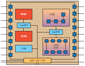
Fig. 3. LogicVision's icBIST contains design objects–the memBIST
and logicBIST controllers–that link to the 1149.1 TAP controller to
provide multiple levels of controller hierarchy.
Automating the whole process
The overall SOC test strategy will be a schedule of executable intermodule
and intramodule test sets. Execution may be for fault detection only (execute
as many test sets in parallel as fast as possible) or for full diagnosis
(execute each test set singly to isolate the cause of failure).
If each of the major design modules is itself self-tested, an additional
top-level hardware scheduler-and-controller could be inserted to sequence
the self-tests and analyze the responses. If this self-test design object
is itself controlled by the chip's 1149.1 TAP controller, the whole SOC
is hierarchically self-testing. This capability enables the embedded self-test
structures to be reused and makes it possible to detect and locate failures
throughout the life cycle of the product.
Automation tools are necessary for the design of testable SOCs. Module-access
analyzers determine the degree of existing peripheral access and either
augment or add a PA structure. Design-hierarchy analyzers determine module
hierarchy, connect module PA structures, and migrate module-level test
protocols to the top level of the design.
Other tools include intermodule interconnect pattern generators and
associated self-test hardware design objects, and an assembler of overall
chip-level test strategy. In addition, an automatic insertion tool is needed
to create top-level PA structures, whether they be fully compliant with
IEEE 1149.1 or partial implementations of the standard, such as a simple
top-level boundary register without the TAP controller and other 1149.1
structures.
Advertisement


