MCM compactness at pc-board prices
Silicon interconnect technology lets standard chips end up in
conventional packages with chip-to-chip delays below 100 ps
Using semiconductor-processing techniques coarse enough for obsolete
fab equipment, a Silicon Valley startup promises to bring compact multichip
modules to the mass PC market. Costs should be comparable to boards with
the same devices on them, while bandwidth improves dramatically.
Alpine Semiconductor (Campbell, CA) has developed a way of making multichip
modules that eliminates many of the bugbears that have previously restricted
such devices to military and other high-cost systems. The modules, called
Complex ICs, fit into standard IC packages and allow testing of unbumped
die before final assembly.
The chip-to-chip signal paths within the modules are 50-ohm transmission
lines, which permit gigahertz-level edge rates and 0.1-ns chip-to- chip
delays. The cost of the process is said to be comparable to that of the
individual packages it replaces.
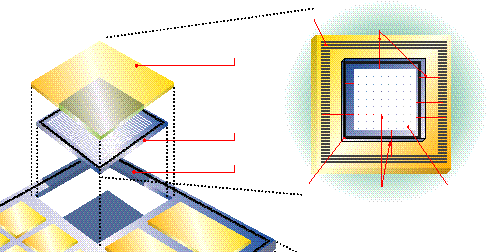
Two kinds of substrates go into the assembly (see figure ). The
larger, called MicroBoard, has holes in it to fit each of the chips. Its
interconnect layer is straight single-layer metal, on the surface. The
traces of this layer go between the holes, and from the outer edges of
the holes to bonding pads at the edges of the substrate.
The other substrate, called MicroPallet, houses all the complexity.
It has four metal layers: X, Y, and ground and power planes. It also has
vias between the X and Y layers, and vias to one surface, where all emerging
contacts receive bumps.
The bumping process is automated, and its cost is independent of the
number of bumps. Therefore there is no cost penalty for wide buses within
a Complex IC. Customizing the MicroPallet for a specific circuit is an
automated one-mask process, with turnaround times comparable to PC boards.
Manufacture of a complex IC starts with bare die, which are neither
bumped nor tested. They are flip-chip mounted on their MicroPallets. Then,
the mounted chips are tested in a jig that connects to the still-exposed
bumps at the periphery.
Complex IC technology combines unpackaged chips into an assembly
that itself can be conventionally packaged as if it were a single large chip.
The tested subassemblies are then flip-chip mounted on the Micro-Board.
At this point the special treatment ends, and the subsystem can be mounted
by standard packaging methods in either a PGA, BGA, or QFP.
Since the MicroPallets are themselves chip size, they can be fabricated
in a semiconductor process. Since the lines are much coarser than current
semiconductors, the processing can take place in old, fully depreciated
facilities.
The starting materials can be reused test wafers or scrap, both much
cheaper than new silicon. Because the chips can be tested before final
assembly, there is no requirement for known good die.
The first known applications appear to be graphics subsystems, with
a graphics accelerator mounted with its frame buffer. ATI (Thornhill, Ontario,
Canada), Atmel (San Jose, CA), and Trident (Mountain View, CA) are all
developing prototypes. For more information from Alpine, e-mail info@alpinemicro.com or
visit http://www.alpinemicro.com.
–Rodney Myrvaagnes
Advertisement


