CMOS sensor array directly registers
fingerprints for personal-ID apps
A working microchip prototype has been developed by SGS-Thomson Microelectronics
(Lincoln, MA) that is capable of directly registering fingerprints for
digital processing in personal-identification applications. The CMOS chip
is a 200 x 200-element sensor array that detects variations in electrical
fields running along the ridges and valleys of fingers without the use
of mechanical or optical adapters.
The company has spent several years developing silicon sensors that
can generate fingerprint images through direct contact. Although the concept
of fingerprint imaging is not new, the semiconductor maker believes that
it is the first to report a working unit that can produce an electrical
representation of a fingerprint.
The chip's architecture is integrated in standard two-metal digital
CMOS technology. It comprises an array of cells that are addressed in a
raster mode with horizontal and vertical scanners and also includes on-board
timing controls and voltage references.
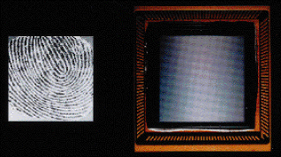
This CMOS chip fingerprint-imaging sensor directly registers variations
in electrical fields running along the ridges and valleys of fingers
without mechanical or optical adapters.
Based on a feedback-capacitive sensing scheme, the device's cells each
include two metal-2 plates assembled adjacent to each other that are separated
from the finger surface by a silicon-oxide layer. The surface to be touched
by the finger is parallel to the two metal-2 plates and separated by a
dielectric and air layer that has a variable thickness.
This structure represents a two-series-connected capacitor scheme. Both
metal-2 plates are individually connected to the input and output of a
high-gain inverter, creating a charge integrator.
To work, the input and output of the circuit is shorted until the inverter
settles into its logical threshold. Next, a fixed charge is sinked from
the input to cause an output swing that is inversely proportional to feedback-capacitance
value. For a fixed sink charge, the inverter's output voltage will range
between two extremes depending on feedback capacitance.
If no feedback capacitance is present, the output voltage will be at
the upper-saturation level, however if the feedback capacitance is large
it will be at a level close to the logical threshold. Because the capacitance
is inversely proportional to the fingerprint distance, a linear output
voltage is produced for electronic imaging of the sampled fingerprint.
The current imager is able to capture at 390 dots/in.for high-reliability
matching based on image-processing algorithms. At an image rate of 10 frames/s,
power consumption is 250 µW for the digital circuitry and 300 µW
for the cell array and buffer. The complete chip consumes less than 1 mW
at 5 V.
Compared to other currently available personal identifcation methods
such as infrared and retinal scans, this single-chip sensor offers improved
security, ease of use, and an improved price/performance ratio. It is also
offered as generating a higher image quality than most identification methods,
including those based on heat.
Future prototypes are expected to increase resolution to 720 dpi. For
more information, contact Amdre Dostie of SGS-Thomson Microelectronics
at 617-259-2517 or e-mail amdre.dostie@st.com .
Advertisement


