How to increase ADC converter speed and resolution while reducing pin count
BY TED HARRIS
National Semiconductor
Santa Clara, CA
http://www.national.com
In today’s world of electronic design, analog-to-digital converters (ADCs) play a pivotal role in translating real-world signals to digital representations. These digital signals are processed and manipulated to perform a variety of operations within a typical system.
For high-speed ADCs, two innovation trends have pushed the technology along over the past few years. First, higher conversion rates are always needed. A wider signal bandwidth can be captured if the ADC samples and converts signals faster. Second, there is the drive toward increasing converter resolution. Increasing the number of bits within a converter improves characteristics such as signal-to-noise ratio and dynamic range. These two goals have worked together to drive the data bandwidth to ever-increasing levels.
Reduced form factor
A continuing industry focus toward smaller physical layouts, has also, among other things, caused industry pressure to reduce component package size. In a monolithic IC, such as an ADC, this almost always means reducing pin count. At first glance, it would appear that the first two goals increased converter speed and increased converter resolutionwould lead to a direct conflict with the third goal of reduced form factor, specifically reduced pin count. Fortunately, there is a solution that can accommodate all three goals: by returning to serial data interfaces.
Serial data interfaces
Serial data interfaces are nothing new. RS-232 has been an industry standard for decades. In the back of the mind of every board-level designer, however, is the latent assumption that parallel data structures will always be faster than serial data structures. While this is true when one compares a parallel data structure and a serial data structure of like type (a parallel CMOS output stage will tend to have higher available bandwidth than a serial CMOS output stage). Every now and then, technology advances enable a leap forward in serial data structures that allow similar data rates in comparison to the existing parallel data formats available. National Semiconductor, the company which defined and introduced Low Voltage Differential Signaling (LVDS), is now using that technology to offer converter technologies with increased converter speed, increased converter resolution, and smaller package sizes by employing LVDS-serial data output structures.

High-speed benefits
There are several advantages to employing LVDS high-speed serial data interfaces to transmit data from the ADC to the digital receiver. First and foremost is pin count. In a traditional parallel CMOS output stage, each digital bit requires a dedicated pin. One additional pin is required to convey timing information by providing the “data-ready” signal. In using a high-speed serial LVDS interface, two pins are required per signal. The signals of note are data, clock, and an additional timing signal, the frame signal, which indicates the boundary between digital words. Since LVDS requires two pins per signal (a positive and a negative signal), a total of six pins is required, even for a 14-bit converter signal.
Using high speed serial interfaces also brings additional benefits. One of the biggest challenges in the board layout stage for most designs is routing the parallel CMOS data lines. The difficulties arise from the sheer number of lines to be routed as well as noise considerations, such as reducing both interference and crosstalk across data lines. Another consideration is limiting the impact these high speed data lines will have on adjacent circuits.
By employing a serial data format, only three differential traces need to be routed, greatly simplifying the layout and reducing the amount of board space dedicated to data traces. Finally, the differential nature of LVDS confers noise immunity. The data line itself experiences a great reduction in common mode noise. In addition, the complementary fields generated help to reduce the EMI created by the high speed data and clock traces into other portions of the circuit. This reduced EMI translates into smaller distances required between components in order to minimize crosstalk, resulting in reduced circuitry size.
Challenges
There’s an old saying: “There’s no such thing as a free lunch.” Nowhere is this truer than in the world of modern electronics. There are challenges raised by the use of high-speed serial LVDS data interfaces. Fortunately, these challenges are already understood and adequate strategies have been developed to mitigate these negatives. Specifically, there is a speed limitation to LVDS drivers. A 14-bit converter running at 105 Msample/s would require a bit stream at 1,470 Mbits/s. Even a well designed LVDS driver cannot be expected to reliably work much beyond 1,100 Mbit/s, at least not over any meaningful trace length.
Another problem is more architectural in nature. Typically, an ADC samples signals, converts them into digital representations, and then sends this data to a processor (an FPGA, a DSP, or in some cases an ASIC). With some notable exceptions, almost all digital processors are parallel in nature. There is a fundamental discrepancy between the format of the data coming out of the ADC and the expected nature of the data at the receiver.
The speed question is not trivial. Without addressing it, ADCs with serial data interfaces would be limited in conversion rate, resolution, or possibly even both. However, using multiple data lanes is one method that avoids this limitation. By adding a second data signal, the bandwidth required of each LVDS driver is reduced by half at the cost of two additional pins.
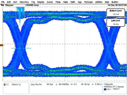
This method is employed in the ADC14DS105, a 14-bit converter capable of sampling data up to 105 Msamples/s. The eye diagram for one of the output drivers (see Fig. 1) is shown with the driver running at close to its maximum rate of 1,120 Mbit/s.

Fig. 1. ADCs such as the 14-bit ADC14DS105, add a second data signal so the bandwidth required of each LVDS driver is reduced by half at the cost of two additional pins. O
This approach is scalable. Once the total bandwidth requirements exhaust the capabilities of even the dual data-lane approach, additional data lanes can be added to further reduce the bandwidth load placed on any single output driver.
The question of how to get a serial data output ADC to communicate with a parallel processor can be tackled with the addition of a functional block, specifically, a deserializer block. While some standalone chips can execute the function, it is entirely plausible to include this function into the FPGA used as the digital receiver.
Many FPGA manufacturers include this standard function in their toolbox. National Semiconductor has code available for the Xilinx Virtex-4 platform that it distributes free of charge. Similarly, many DSPs are beginning to include data input structures that will accept high-speed serial data and deserialize the data internally. As for ASICs, including a deserializer block in the next revision would be a relatively simple matter that should not significantly contribute to the overall die size.
True, challenges exist to employing a high-speed serial data interface for transmitting data from the ADC to the receiver. But for those applications with the flexibility to employ some additional functional blocks, the rewards may be great. The ability to deliver simultaneously on the often times competing goals of higher converter speed, greater converter resolution, and smaller physical layout sizes is indeed valuable enough to make it worth consideration.
Advertisement
Learn more about National Semiconductor


