EDA happening – New process builds CMP models
XYALIS (Grenoble, France) a design for manufacturing and layout finishing software company has announce that thanks to “non destructive” nanometric measurement equipment’s, they are able to build Chermo Mechanical Planarization (CMP) models. These models are used for estimating the critical areas where dummy filling is needed to smooth the thickness variation.
Building a model is a complex process that must be qualified by “non destructive” measures on production chips. These measures help to analyze the layers thickness and fine tune the model.
Accomplished with the partership of XYALIS and CIME-Nanotech (Minatec Research Center) in Grenoble , it will allow XYALIS to provide high accuracy thickness measurements on wafers.
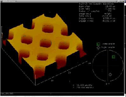
All the requested data to build these models can be obtained with an Atomic Force Microscope (AFM). With a resolution possibly going to less than 1 nm,accuracy is no more a challenge.
XYALIS GTsmooth, density estimator and tiling engine, uses such model.With these measures, XYALIS will reduce the time needed in building aspecific model.

3 D view of grid metal deposition
Advertisement
Learn more about Electronic Products Magazine


