Test system automates on-wafer power device measurements
Until this year, if you wanted to characterize the power performance of an IC, you first had to package it and, if it didn’t work, you not only wasted precious design time but the cost of the package as well. Specifically designed for on-wafer characterization of power devices, the Tesla test system (see Electronic Products , July 2007, p. 104), lets users perform complete overtemperature low-contact-resistance measurement of devices up to 60 A and 3,000 V.
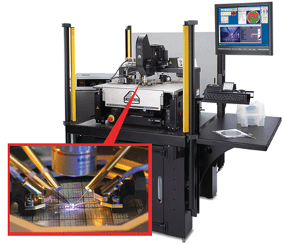
To do that, the test system’s designers had to come up with two new kinds of probes and a new type of chuck to hold the wafer. Designed for RDS(on) measurements, the High Current Parametric (HCP) probe minimizes thermal runaway at the probe-to-wafer contact while supporting up to 10 A in continuous mode and up to 60 A in pulsed mode, while the High Voltage Parametric (HVP) probe enables breakdown-voltage measurements as low as 1 pA at 3,000 V. The Vacuchannel chuck technology provides not only state-of-the-art handling for wafers as thin as 100 μm, but also on-wafer measurements to 75 W.
Cascade Microtech , Beaverton , OR
Information 503-601-1000
Advertisement
Learn more about Cascade Microtech


