Power supply feedback, protection on one chip
Control and isolation of a power supply typically requires multiple components. Here’s how it can be implemented on one chip
BY GEORGE RASKO
ASIC Advantage
Sunnyvale, CA
http:\www.asicadvantage.com
Controlling the voltage and current for the output of an isolated power supply for a particular load typically involves sensing the output voltage and current. This information serves as feedback to the primary-side engine of the power supply. The functional elements of this include stable voltage references, gain elements to amplify the difference between a reference and sensed voltage, and a buffer from the error amplifier output to drive the signal across the isolation boundary in the feedback path to the primary-side controller. Depending on the application, one aspect of the output will be regulated, with protection implemented for the other, such as over-voltage for a no-load event or over-current in a short-circuit condition. Rather than implement each function with separate components, a chip integrating these elements can be used to serve these requirements in a number of different configurations.
Power supplies
In a typical power supply, the desired output is a constant dc voltage, where the output voltage is divided through a resistor network that scales the output voltage to be input into a differential error amplifier. One input of the error amplifier is the divided-down output voltage, with the other input to the error amplifier being a constant voltage reference. The dc gain of the amplifier is high, and in closed loop operation, the output of the amplifier generates an error signal dependent on the regulation of the output voltage. In an ac/dc power supply, the sensing is normally done on the (isolated) secondary side, while the main control function is implemented on the primary side. The power conversion electrical isolation is accomplished through a power transformer, while the feedback signal is normally isolated optically.

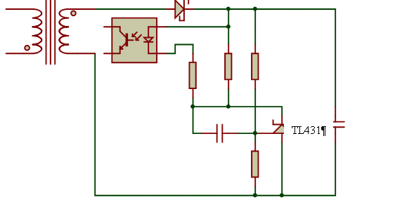
Fig. 1. TL431 typical power supply implementation.
A typical output measurement and reference component is the TL431, available from several manufacturers. The TL431 contains a voltage reference and a trans-conductance amplifier, using the amplifier output as the power input for internal circuitry. It can be used for voltage control, with the current controlled output used to drive the photodiode of an optocoupler. A typical power supply circuit with the TL431 is shown in Fig. 1 , along with necessary bias resistor and a compensation capacitor. Provision of additional secondary protection functionality at this point becomes much more complicated, requiring a variety of additional components. The higher value of the TL431 and similar components are less useful for this function due to their higher reference voltages, which impacts sensing in general as well as the ability to “pull-down” on the feedback signal below the internal voltage, (typically 2 V with the TL431). Primary-side protection schemes can provide some protection, but typically they are insufficient due to noise and delayed reaction to secondary based fault events.

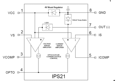
Fig. 2. IPS21 functional schematic.
A more complete solution should provide more functionality, such as dual sensing elements. Examples of this are the IPS20 and IPS21 from ASIC Advantage (see Fig. 2). These feedback and protection ICs include a voltage control element, as well as a dedicated error amplifier for current measurement with a reference voltage set at a more advantageous lower value. The outputs of the two amplifiers are combined by a buffer circuit, configured to drive an opto-coupler in a source versus sink configuration. This mitigates the down limits as typical in the shunt only configuration of the pure trans-conductance circuits such as the TL431. The IPS21 has an internal reference of 100 mV, which allows the use of a current sensing resistor of a much lower value, dissipating lower power for improved efficiency. The device uses a Zener-like shunt regulator for power, requiring only a single resistor for pull-up to a secondary voltage.
Resistor-less sensing
In some applications, providing a low-value current sensing resistor is a concern due to efficiency or space. A feedback and protection component such as the IPS20 provides a solution to this dilemma by allowing the use of a PCB copper trace as a current sense resistor. The IPS20 is functionally identical to the IPS21, except that the 100 mV constant voltage reference is replaced by a nominal 50 mV reference that increases with temperature (referred to as PTAT, proportional to absolute temperature).
Resistor manufacturers expend considerable engineering effort to provide components that don’t vary with temperature. Plain metals like copper, which is used to make the traces on PCBs, have a resistance that varies with temperature, but this variation is predictable. To get accurate sensing over a range of temperatures, it is necessary to compensate for this resistance variation. The IPS20 implements this variation as an internal function, enabling the designer to focus on other aspects of the application. A typical value quoted for the temperature coefficient of resistance of copper at room temperature is 0.00393/°C (this value varies with whether the copper is pure annealed, cold worked, or has trace impurity levels). For a 50 mV nominal reference, the ideal slope of a plot of the reference voltage with temperature is 50 mV x 0.00393 = 0.1965 mV/°C. AAI’s datasheet nominal value of this slope is 0.16 mV/°C, with measured values a bit higher (around 0.18 mV/°C).
On PCB traces, a typical PCB may use 1 oz copper, about 0.0014 in. thick (35 µm). A hot air solder leveling (HASL) coating is around 300 µin. of solder. This corresponds to a vertical thickness for the PCB trace of 0.0017 in., with about 82% copper. Tin has a volume resistivity of 11.5 µΩ-cm, 6.7 times copper, while lead is 22 µΩ-cm, 13 times copper. This means trace resistance is dominated by copper, despite a protective tin-lead coating. (Note also, the temperature coefficient of resistance for tin is 0.0042/°C and lead is 0.0040/°C, both very close to that of copper.)
Considerations in optical feedback
To help prevent unexpected or unwanted results, a few implementation hints about feedback current are helpful. Many primary side PWMs have low feedback current requirements. This is done to keep down the startup and operating power in the chip. The current through the opto-coupler must meet the manufacturer’s requirement for a specified current transfer ratio (CTR). Be aware that the CTR and bandwidth of most opto-couplers drops with reduced operating current.
LED driver application
LEDs operate best when driven by a constant current. At a fixed current, their voltage drop has an initial tolerance, as well as variation with temperature. When more than one LED needs to be driven, it is typical to put them into a series string and then drive the string at a fixed current. It is straightforward to implement current feedback to a power supply to provide this drive. There needs to be output protection in case one of the LEDs fails in an open circuit condition to prevent the output voltage from growing to excessively large values. The IPS21 can implement these two functions, allowing the current amplifier to control the feedback during normal operation and use the voltage channel to implement open-LED/overvoltage protection. An example of this is shown in Fig. 3 .

Fig. 3. IPS21 LED driver schematic.
Battery charger application
Charging a secondary battery is often done in a constant current manner. The desired charging profile (the desired charging current versus battery voltage) varies with battery chemistry and application. The same idea as shown above as an LED driver can be used as a battery charger. The charging current is set by the current sensing resistor and the shutoff voltage (the voltage at which the charging current should go to almost zero) is set by the resistor divider. The basic circuit has two states: it is either providing constant current or is shutdown. More complex schemes can be implemented using additional resistor dividers off the output feeding into the current sensing (to slowly bring down the charging current as the battery voltage increases), or thermistors to limit charging if the battery or ambient temperature is above a certain value.
References
1. Application notes and IPS20 and IPS21 datasheets from www.in-plug.com
2. Reference Data For Radio Engineers, Resistivities Of Metals And Alloys
Advertisement
Learn more about ASIC Advantage


