Assembling the Tessera OptiML Wafer-Level Camera
In the mid 2000s, Tessera Technologies CEO Bruce McWilliams had a vision of where cell phones and the digital optics technology inside of them were going. But the state-of-the-art in camera modules for portable electronics didn’t fit with high-volume fab lines that made such devices possible.
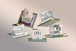
Tessera’s OptiML wafer-level camera
At the time, camera modules were usually being made using more-or-less traditional packaging and lens optics, which meant that they couldn’t be handled, placed, or added to boards in the same way that traditional semiconductor devices were. As a result, they required special, more costly assembly techniques.
Bruce was not a newcomer to the electronics industry. In his 20-year career in the semiconductor industry, he had served as an executive and technical manager, including senior vice president at Flextronics International, a position he assumed when Flextronics acquired nCHIP, a multichip module and IC packaging company he co-founded, as he had S-Vision, a silicon chip-based display company.
His understanding of packaging issues led him to Israel-based Shellcase Ltd., which had developed a way to commercially package image sensors at the wafer level. In November 2005, Tessera agreed to pay approximately $33 million in cash for Shellcase’s packaging intellectual property. Xintec in Taiwan and China WLCSP are currently licensed subcontract package sources for Tessera’s SHELLCASE technology.
The optics solution
But having wafer-level packaging for image sensors wasn’t sufficient — optics were needed as well. The answer to this state-of-the-art problem came from Digital Optics Corp. to manufacture micro-optics, initially for the military. In July 2007, Tessera acquired Digital Optics.
An important piece of the puzzle were the algorithms needed to enhance image quality. This work was done by EyeSquad, which was acquired by Tessera in February 2007.
With all the essential elements in hand, Tessera was beginning to create a consumer-optics one-stop-shop for wafer-level camera (WLC) solutions — which, like your average semiconductor device, could be handled and reflow soldered in high-speed production lines. In mid 2007, it released the OptiML WLC technology to the market.
Richard Comerford
Advertisement
Learn more about Tessera


