The right ESD protection goes beyond datasheet specs
BY JOE SALVADOR
California Micro Devices, Milpitas, CA
http://www.cmd.com
http://www.XtremeESD.com
The adoption of high-speed serial data interfaces and the move to smaller semiconductor manufacturing geometries is necessary for cost, integration, and performance factors, but this smaller geometry is also more prone to ESD damage at lower voltage and current levels. Additionally, low-capacitance ESD devices required on high-speed data lines tend to have higher dynamic resistance as their capacitance decreases, making them less capable of protecting sensitive ICs in the system.
With traditional ESD protection, an inverse relationship exists between robust ESD protection and good signal integrity. Some ASICs have no acceptable traditional ESD device that can provide required ESD protection levels combined with acceptable signal integrity.
Datasheet specifications
System designers often compare ESD protection devices using device datasheet ESD-level ratings. These ratings only guarantee what the ESD device, not what the system, will survive.
A device rated for 8 kV can fail a system-level test at 2 kV or lower. In other cases, a device rated for 15 kV may not protect a system as well as an 8-kV rated device. This primary parameter that most system designers use to compare ESD devices gives no indication of the actual system-level performance.
System ICs can be damaged by excessive voltage, excessive current, or both. Many system designers are aware that excessive voltage can damage an IC, but are unaware that high current levels are often the real cause of ESD damage.
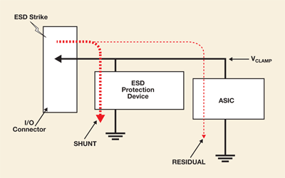
Fig. 1. In traditional ESD protection architectures, an inverse relationship exists between protection and signal integrity.
ESD protection devices function by shunting most of the current to ground and “clamping” the voltage seen at the ASIC to a lower value than the strike voltage. Ideally, the way to compare ESD devices is to examine their clamping voltage and residual current (the current that does not get shunted through the ESD device). However, this is easier said than done.
Clamping voltage
The clamping voltage quoted in most ESD protection datasheets can be misleading. Current industry practice is to publish clamping voltages based on a pulse with an 8-µs rise time and duration of 20 µs.
Most datasheets document clamping voltage using a 1-A pulse and sometimes a higher-current pulse as well. This pulse is used because it is repeatable and easy to measure. Unfortunately, this pulse is not equivalent to an ESD pulse, which has a 1-ns rise time and a duration of 60 ns. Also, the clamping voltage during a level 4 IEC 61000-4-2 strike with a peak current of 30 A is much different than seen during a 1-A pulse.
Using the standard 1-A pulse, most semiconductor ESD protection diodes are rated to clamp between 8 and 15 V. Confronted with an 8-kV IEC 61000-4-2 strike, these diodes typically show peak clamping voltages of 50 to 100 V, depending on other diode characteristics such as dynamic resistance.
Some ESD vendors also include ESD pulse waveforms, but these can also be misleading. For example, vendors typically use attenuators to keep from damaging their test equipment. When shown on a waveform plot, the clamping voltage in the datasheet often does not show the impact of the attenuator, misstating the clamping voltage by a factor of 5 to 10 times.
Although it is not possible to compare ESD performance solely using the clamping voltages shown in most datasheets, there are ways to compare relative performance by reading the datasheet carefully.
Other considerations
The clamping voltage seen by the protected ASIC is based on several factors, including the breakdown voltage of the ESD diode, the dynamic resistance of the diode, and the amount of current flowing through the diode. While the clamping voltages on datasheets using an 8/20–µs pulse are not equivalent to an ESD pulse, they can be used to compare devices — if done properly.
A simplified model of clamping voltage is that it increases linearly with the current. The line’s slope is the diode’s dynamic resistance.
Most ESD devices publish a 1-A Vclamp and a value for dynamic resistance, or two values for Vclamp at different current levels, making calculating dynamic resistance relatively straightforward. For example, a device with a clamp voltage of 10.0 V at 1.0 A, and a clamp voltage of 15.0 V at 5 A would have a dynamic resistance of (15 – 10)/(5 – 1) = 1.25 Ω.
Dynamic resistance is the most important factor in determining the actual clamping voltage. Consider two devices: device A, which has an 8-V clamp at 1.0 A, and device B with a 10-V clamp at 1.0 A. Which one is better during an ESD strike?
The 8-V clamp may seem better, but this may not be true. If device B with the 10-V clamp has an Rdyn of 1 Ω, and device A with the 8-V clamp has an Rdyn of 2 Ω, then the 30-A clamp voltage for device A is 8 + 29 * 2 = 66 V, while device B is 10 + 29 * 1 = 39 V, making device B much better.
The amount of current flowing through to the ASIC also depends on the dynamic resistance through the protection circuit. As resistance increases, the current flowing through the protected device increases proportionally, and with it the likelihood of ESD damage.
The designer should choose a protection device that shunts as much current as possible and minimizes the residual current seen at the ASIC. Because this current is system dependent, it is not typically specified in datasheets. Unfortunately, very few ESD protection vendors specify dynamic resistance either, but the values can be approximated from the listed clamping voltages.
Generally, ESD diodes have dynamic resistance in the range of 1 to 3 Ω, while other devices such as varistors and similar suppressors tend to have dynamic resistance in the range of 20 to 40 Ω, making ESD diodes the preferred ESD solution.
Traditional ESD protection
As shown in Fig. 1 , a traditional, single-stage ESD protection device performs the following actions when a strike occurs: (1) The voltage is clamped to a lower voltage to minimize the voltage seen at the ASIC. (2) The protection device shunts current to ground and away from the protected ASIC. (3) Once the ESD strike is fully dissipated, the protection device attempts to return to a high-impedance state. Some devices, such as polymers, can take over 24 hours to return to this state so it is important to understand this characteristic.
Reducing the dynamic resistance through the ESD protection device will reduce the clamping voltage and also reduce the residual current seen at the ASIC. With the increased sensitivity of the latest ASICs, there are many production ASICs already for which NO traditional ESD device will provide adequate protection.
New solutions
Solutions such as CMD’s PicoGuard XP feature a novel dual-stage design that places two ESD protection stages and a resistor in series within the same package to reduce the current reaching the ASIC. During an ESD strike, this solution works as follows:
1. Stage 1 of the architecture begins to clamp. Stage 1 residual passes through the series resistor and enters into the second stage.
2. The majority of Stage 1 residual is shunted away from the conducting path leading to the ASIC in stage 2, dramatically reducing the current seen at the ASIC as compared to single-clamp protection architectures. The clamping voltage is similarly reduced using this two-stage clamp.
In one example, the survivability of an ASIC went from less than 6 kV using a traditional ESD diode solution to greater than 10 kV with the CM1231, the first device to incorporate the PicoGuard XP architecture.
For more on circuit protection, visit http://www2.electronicproducts.com/Passive.aspx.
Advertisement
Learn more about California Micro Devices


