Evolving power transistor meets changing needs
Leveraging the high power density of a vertical transistor, RF power transistors promise performance for modern RF apps
BY BRIAN D. BATTAGLIA
HVVi Semiconductors
Phoenix, AZ
http://www.hvvi.com
While it is often overlooked, the steady evolution of the power transistor has played a key role in the successful development of a wide variety of applications from avionics and radar systems to cellular communications and satellite TV. All these markets would not exist today were it not for the availability of high power, high efficiency and low-cost silicon power transistors.
Driving that success has been steady and timely technological advances. Early development of power transistors for RF applications in the 1950s and 1960s, for example, centered primarily on the military where developers were first drawn to germanium. Those devices were quickly replaced by bipolar components that offered high power in a cost-effective silicon fabrication process.
As performance demands increased in the 1970s and early 1980s, developers responded with power transistors developed in silicon DMOS (double-diffused metal oxide semiconductor). Using a vertical transistor design, this approach allowed designers to develop power transistors capable of operating at supply voltages up to 50 V and 500 MHz. The technology’s inherent advantages offered designers fast switching response, better thermal stability, and higher impedances.
Wireless comm needs
By the 1990s as communications equipment manufacturers began to build out the wireless communications infrastructure, system designers demanded higher-efficiency power amplifiers (PAs). Basestation manufacturers needed PAs capable of offering higher linearity to satisfy higher-order modulation schemes, greater average output power levels, broader operating bandwidths, and helping reduce operating costs by decreasing basestation energy consumption.
While DMOS offered a number of advantages, as frequencies pushed past 500 MHz, the technology performance was limited. In response to this need, semiconductor developers introduced LDMOS (lateral double-diffused metal oxide semiconductor) architecture in silicon and compound semiconductors such as gallium nitride (GaN) HEMTs. These new technologies offered better gain and third-order intermodulation distortion (IMD3) over a larger dynamic range than traditional DMOS devices.
Constantly escalating performance demands continue to drive power transistor performance requirements to new heights. An excellent example is in the avionics and radar markets where performance demands are driving development of pulsed radar applications in the L band.
Designers of ground-based radar operating in the 1.2 to 1.4-GHz band, for instance, need to boost the range and sensitivity of their systems to allow air traffic controllers to better manage higher levels of air traffic. New applications, such as the Automatic Dependant Surveillance Broadcast system (ADS-B), use GPS data to identify the location, speed, and direction of the aircraft and to communicate with other aircraft to allow the pilot to alter course to shorten travel time and reduce fuel consumption.
In all of these applications equipment designers need power amplifiers capable of delivering higher levels of output power at higher efficiency and with higher linearity to reduce costs. At the same time, designers building new avionics and radar systems, particularly those mounted in aircraft, are under intense pressure to reduce the size, weight and power consumption of their subsystem.
Meeting these needs with existing power amplifier technologies forces designers to make significant compromises. Bipolar devices deliver relatively high voltage levels, but at low gain. LDMOS components offer better gain, but limited ruggedness.
Furthermore, power transistors manufactured in LDMOS hit a ceiling as they exceed 3.0 GHz. Some system designers have turned to power transistors fabricated in nonsilicon technologies, such as gallium nitride or silicon carbide, to achieve higher performance. But these more exotic compound semiconductor technologies can’t match the cost advantages of widely-deployed silicon.
Higher power, higher voltage
Last year saw the first new breakthrough in silicon-based power transistor design in over 15 years. Developed by engineers at HVVi Semiconductors, the new architecture employs a high-voltage vertical field effect transistor (HVVFET) to bring higher power through voltage.
By reducing parasitics, this new process technology offers an improvement in frequency bandwidth over LDMOS. Moreover, by taking advantage of the higher power density of the vertical transistor over the lateral transistor used in LDMOS, products based on this new process can offer twice the power in the same package.
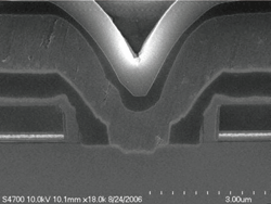
Fig. 1. Cross-section of HVVFET architecture that employs high-voltage to obtain more power.
One key to this architecture’s unique characteristics is its ability to scale to higher operating voltages. The substrate of an HVVFET acts as the drain of the transistor. The device depletes vertically into the substrate as voltage is applied to the drain.
The architecture approaches planar breakdown in the vertical drain region and thereby stands off the maximum voltage with the minimum RDS(on) . At the same time, the architecture maximizes packing density while minimizing parasitic capacitance.
The performance characteristics of this unique structure improve as the device moves to higher operating voltages. As operating voltage increases, the required drain-source current of the device decreases. This allows power transistor designers to reduce die size and decrease parasitic capacitance-per-watt. Lower capacitance supports higher frequency operation and lower current density leads to improved reliability.
Moreover, while individual HVVFET-based components offer improvements in output power, gain, efficiency and ruggedness, the technology’s most dramatic advantages come at the system level. By significantly boosting gain, HVVFET-based power transistors can be used to reduce drive stage requirements.
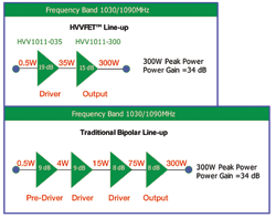
Fig. 2. Comparison of existing bipolar or LDMOS RF power transistors to HVVFET-based transistors.
Figure 2 , for example, depicts a traditional 600-W solution using existing bipolar or LDMOS RF power transistors. Using HVVFET-based power transistors, designers can build the same 600-W solution with a simpler two-stage design.
The new design offers multiple advantages. By delivering 300 W of output power at 30% higher system efficiency, the two-stage design helps reduce system power supply requirements and operating costs. Also, by reducing the number of components, it reduces PCB footprint by 50% and drives down system costs.
■
Advertisement
Learn more about HVVi Semiconductors Inc.


