ESD protection design for discrete semiconductors
Some companies require inclusion of ESD protection on discrete components but it can be challenging
BY DONNA ROBINSON-HAHN and STEVEN SAPP
Fairchild Semiconductor
South Portland, ME
http://www.fairchildsemi.com
Electrostatic discharge (ESD) is caused by the discharge of an excess or deficiency of electrons on one surface with respect to another surface or to ground. When a static charge is present on an object, the molecules are electrically imbalanced.
ESD occurs when equilibrium is attempted via the transfer of electrons between one object and another that is at a different voltage potential. When an ESD-sensitive device, such as a MOSFET or other discrete component, becomes part of the discharge path or is exposed to an electrostatic field, it can be permanently damaged.
ESD damage is thermal in nature, resulting in melted material or dielectric rupture due to excess electric field. Hence, ESD protection measures involving on-chip ESD protection structures or ESD enhanced fabrication processes are usually the first line of defense.
ESD protection optional?
While on-chip ESD protection circuit design has been an integral part of development of almost every single IC chip, inclusion of such protection on most discrete components has been considered optional by many semiconductor and system manufacturers using these products in their systems. ESD-protected versions of discrete components are available, but minimal risk of ESD damage due to the ESD protection measures used during manufacture and an appropriate PCB design mitigating ESD damage to the discrete component, coupled with demand for low-cost components with high volume most often results in the purchase of unprotected discrete components.
For a variety of reasons, there has been a recent move by some large system manufacturers to require inclusion of ESD protection on discrete components designed into their systems. Just as with ICs, ESD protection of some types of discrete components can be challenging.
ESD sensitivity in MOSFETs
For MOSFETs, the gate oxide between the gate and channel using modern CMOS processes is extremely thin resulting in varying degrees of ESD sensitivity. The electric field Eox across the gate oxide of thickness tox when voltage V is applied is Eox = V / tox .
For very small tox , the electric field Eox can exceed the breakdown field Ebk for relatively small voltages.1 ESD damage of the MOSFET occurs when the gate-to-source voltage is high enough to damage the gate dielectric.
A leakage path through the gate oxide can result in a catastrophic failure. Besides the MOSFET, IGBT power modules are also sensitive to ESD because the thickness of the gate isolation is on the order of 100 nm.
The degree of sensitivity also depends on the input capacitance value. IGBTs and power MOSFETs with large chip areas are characterized by high input capacitances. As a general rule, the proportionality between the die area and ESD threshold of the component, such as an LVMOSFET (low-voltage MOSFET), is relatively predictable based on the capacitance ratio between the MOSFET and the forcing capacitor in the ESD circuit.
Failure occurs when the voltage across the gate oxide forces sufficient current to disrupt the gate oxide. Thinner gate oxide can actually improve the human body model (HBM) threshold in some scenarios because input capacitance increases and reduces the stress on the oxide by increasing its magnitude compared to the forcing capacitor.
Protecting MOSFETs
To protect a MOSFET from ESD or any other excess gate voltage, the primary objective is to keep the gate-to-source voltage from exceeding the breakdown voltage. In order to achieve this, ESD protection:
May be required at all gates to prevent damage during fabrication.May also be required at all input/output pads connected to a sensitive region.May include shorting the gate to the source or applying zener protection gate-to-source.May be a function of gate-to-gate spacings.2 Usually increases gate leakage.Can increase die size by up to 10%.Can be as simple as reversed biased diodes (see Fig. 1 ) where the diode network prevents VGS from exceeding the oxide breakdown voltage.3 Diodes should be tied to voltages according to the MOSFET Vgs and large voltages across the gate oxide should be avoided.3
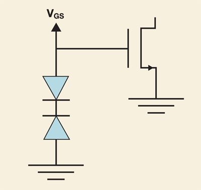
Fig. 1. ESD protection for MOSFET gates.
Human-body model
Before we can consider the type of protection required during the design of a discrete component, we must first understand the various types of ESD. Humans are a principal source of ESD, characterized by the HBM. This is the most commonly used model to describe an ESD event.
This model represents the discharge from the fingertip of an individual to a device. From an ESD perspective, the event is rather slow, measured in nanoseconds, and is modeled by a 100-pF capacitor discharged through a switching component and a 1.5-kΩ series resistor into the device under test (DUT).
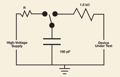
Fig. 2. A typical HBM circuit.
Charged-device model
The charged-device model (CDM), on the other hand, represents a discharge from a device rather than to it (see Fig. 3 ). If a device becomes charged (for example, sliding down a feeder or plastic tube) and then is discharged by coming in contact or close proximity to a conductive surface, a rapid discharge occurs from the device to the conductive object.
The amount of charge stored in a CDM event is very dependent upon the package capacitance and as such smaller packages lend themselves to higher resistance to CDM events. In contrast to HBM, the CDM rise time is determined by the parasitic inductance, capacitance and resistance and is very fast.
Although we cannot determine the CDM peak current very easily, it could be as high as 10 A for a 500 V CDM pulse. Most of the charge is stored in the VDD and ground node because the power and ground planes typically have the largest area within the package. CDM is also not limited to I/O pins. For some device types, this type of event can be more destructive than the HBM event.

Fig. 3. A typical CDM test circuit.
ESD damage
According to most recent studies, less than 10% of all documented damage actually came from ungrounded personnel touching ESD sensitive products (HBM). The most common form of ESD damage is reportedly CDM. Although CDM is arguably the leading cause of ESD damage among electronic components, some semiconductors, including discrete components, are neither tested for CDM sensitivity nor required to meet any minimum CDM threshold.
Unlike HBM, CDM sensitivity involves not only the component design, but also the package capacitance. Small six-lead components usually have very high resistance to CDM events with CDM protection thresholds up to 2,000 V.
Larger packages and components can hold a much higher voltage, resulting in CDM sensitivities of less than 300 V, with the current industry “standard” for CDM for most semiconductors set at 500 V. Discrete components are generally housed in packages just large enough to contain them and large die that are less sensitive to ESD damage due to large capacitance are found in larger packages. Studies by Fairchild on discrete MOSFET components generally show relatively high CDM performance in excess of 500 V.
Protecting components from the effects of ESD damage begins by knowing how they can be damaged and their level of sensitivity. Besides the inclusion of ESD protection at the component level, setting appropriate device requirements by system manufacturers is something that also needs to be carefully considered. The need for ESD protection will vary according to the product type and end application as well as taking into consideration any design limitations or tradeoffs. ■
1.http://www.esda.org/basics/part1.cfm)
2.Voldman, Steve, et al, IBM, IEEE, 1996
3. http://bmf.ece.queensu.ca/mediawiki/index.php/MOSFET_layers_and_layout
For more on ESD protection, visit http://www2.electronicproducts.com/Passive.aspx
Related Products: Diodes, Transistors, and Thyristors
Related Products: Circuit Protection
Advertisement
Learn more about Fairchild Semiconductor


