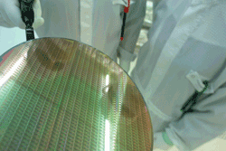
Sensor and CMOS IC integration concept enables smallest form factors
The business unit Full Service Foundry of austriamicrosystems (Unterpremstaetten, Austria) announced the availability of its new technology called Through Silicon Via (TSV) technology which promises foundry customers reduced form factor, systems cost reduction as well as performance improvements due to shortened interconnect lengths. This technology will enable a variety of markets demanding 3D integration of CMOS ICs, photo sensors, gas sensors, power devices, or MEMS components such as automotive, industrial & consumer applications.

With the TSV technology two 8-in. wafers can be electrically connected. With typical TSV depths of 200 to 300 µm, it is especially targeting 3D integration of CMOS ICs and sensor components. A proprietary back side re-distribution layer concept enables various front and back side IO pad connections and provides customers with utmost flexibility in IC and sensor arrangement.
In addition, this TSV technology can be combined with the company’s 0.35µm analog specialty technologies such as CMOS, HV-CMOS, SiGe BiCMOS or embedded nonvolatile memory. For more information, contact Andreas Wild at 011-43-(0)-3136-500-4400 or e-mail andreas.wild@austriamicrosystems.com.
Christina Nickolas
Advertisement
Learn more about ams (formerly austriamicrosystems)


