Mobile functionality with flip-chip packaging
Several factors are driving the demand for flip-chip packaging
BY CRAIG MITCHELL
Tessera, San Jose, CA
http://www.tessera.com/
Smart phones are a rapidly growing share of mobile phone shipments, representing 15% of the market in 2009 and growing to 35% in 2013. Essentially all the growth in mobile phone sales will come from smart phones over the next 4 years. Likewise in computing, all of the growth is in notebooks and netbooks while desktop sales are declining.
As the demand for high functionality in mobile devices grows, so does the need for semiconductor-packaging solutions that meet increasingly complex requirements for performance, miniaturization, and cost reduction. Flip-chip packaging is a key part of the solution for meeting these needs, and a copper pillar substrate approach is particularly well suited for advanced mobile applications.
Several factors are driving the demand for flip-chip packaging, and many of these are related to higher I/O requirements. Baseband and applications processors are seeing I/O counts growing as more functions Internet, GPS, MP3, accelerometers, touchscreens are added to phones. Integration of the memory controller into the CPU increases the I/O count for those devices. Multicore CPUs and multichannel memory also contribute to that trend. High-definition video creates a need for graphics processors in smart phones, netbooks, and games, and these are typically high I/O devices as well.
Meanwhile, migration to flip-chip packaging is supported by a pair of global conditions. First, the high cost of gold for wire-bonded devices has lowered the I/O count at which flip chip becomes more economical than wire bonding. And secondly, new flip-chip substrate capacity has come on line, relieving what has been a supply-chain bottleneck.
The growth of flip-chip interconnect, however, has put the spotlight on several technical issues. With higher I/O counts there is a desire to reduce bump pitch. At pitches less than 180 µm, though, control of solder volume on package substrate pads is very challenging and can result in reduced substrate and flip-chip assembly yields.
Electromigration risk is increased if solder pad sizes on the chip and package are reduced to achieve a tighter pitch, which results in current crowding. When Pb-free solders are used at fine pitch, solder-joint collapse increases stress and lowers thermal cycling reliability, while also making underfilling more challenging. Another emerging approach uses copper pillars on the chip rather than solder bumps, but this is a high-cost process and the pillar structure increases the risk of fracturing fragile low-k dielectric layers being adopted for today’s high-performance semiconductors.
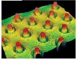
One solution that addresses these challenges uses conventional Pb-free solder bumps on the chip bond pads and a copper pillar contact on the substrate. Tessera’s µPILR substrate (see Fig. 1 ) employs this approach, and the result is a high-reliability structure with numerous advantages. Since the copper pillars are created by etching, the process is scalable to very fine pitch and also results in excellent coplanarity of the contacts.

Fig. 1. The µPILR flip-chip substrate features highly coplanar fine pitch copper posts etched from a copper sheet of very uniform thickness.
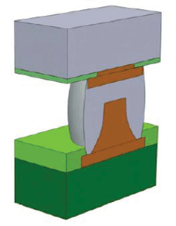
The structure shown in Fig. 2 replaces the troublesome solder on the substrate pad and provides a predictable standoff height for underfilling, even with lead-free solders that can collapse without added support. Because the substrate Cu pillars provide a vertical wetting surface and can be uniformly etched at very fine pitch, the pitch of the solder pads on the chip can be reduced without shrinking the pad size to avoid bridging. This cuts the risk of current crowding and resultant electromigration effects.
Recent electromigration testing of µPILR flip-chip test vehicles with Cu posts at 150-µm pitch shows less than 3% increase in resistance after 1,300 hours of stressing at 1.0 A at 160C. The µPILR flip-chip structure also shows a 20% lower energy release rate in underlying dielectric layers compared with Cu pillar on chip in reliability simulations, and no failures up to 1,000 hours of temperature cycle testing from 55º to 125C.

Fig. 2. The µPILR flip-chip copper post on substrate provides positive standoff for underfill flow and lower stress on low-K dielectric layers than copper pillar on chip.
As we have seen numerous times over the years, the industry will adopt new packaging technology to meet constantly evolving requirements. With consumer mobile applications driving those requirements now, the solutions need to support high pin counts, enable miniaturization, simplify the assembly process, and provide reliability in a mobile environment. A Cu pillar on substrate flip-chip approach such as µPILR meets these needs. ■
Advertisement
Learn more about Tessera


