Selecting and using high-precision D/A converters
Careful attention to various issues is critical
BY CHAD STEWARD and ALISON STEER
Linear Technology, Milpitas, CA
http://www.linear.com
The first step in selecting and using high-precision D/A converters is to consider the DAC architecture that is best for a given application. Several architectures are available, including oversampled, composite, resistor string, and resistive ladder or R-2R DACs. The chosen architecture affects the specifications of the DAC itself and places specific demands on the board designer. Careful consideration of the effects of the performance of the power supply, reference, and output amplifier on the DAC is required to achieve the best performance.
Oversampled or ΔΣ
An oversampled or delta-sigma (ΔΣ) DAC uses a low-resolution DAC, normally just 1 bit, preceded by a noise-shaping digital modulator and followed by an analog low-pass filter. The most accurate commercially available ΔΣ DACs achieve ±15-ppm accuracy, or about ±1-LSB INL at 16-bit resolution, but require 15 ms to settle and suffer a relatively high 1 µV/√Hz noise density. Other available over-sampled DACs achieve settling in 80 µs, but they suffer poor INL of about ±1 LSB at 12-bit resolution.
Composite DACs
It is possible to construct a high-resolution composite DAC by combining two lower-resolution monolithic DACs. A common technique is to use a coarse DAC to achieve the desired range and a fine DAC to achieve the required resolution. Note that since the relationship between the full-scale range of the two DACs is not well controlled, overlap between the resolution of the coarse DAC and the range of the fine DAC is required to ensure that all desired output voltages are realizable.
The accuracy and drift of the coarse DAC typically limits the end accuracy of the composite DAC, so increased precision requires characterization and software correction of the composite DAC transfer function. Frequent calibration may also be required to correct for drift due to variations with temperature, time, humidity, mechanical stress, and so forth.

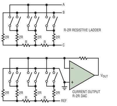
Fig. 1. Resistive ladder DAC structures.
Resistor string DACs
A resistor string DAC uses a series resistive divider with 2N tap points to create a DAC with N-bit resolution. Monolithic 16-bit DACs based on resistor string architectures typically contain a lower-resolution resistor string DAC with one or more subranging DACs used to interpolate between the elements of the string to achieve 16-bit resolution. One advantage of this string-plus-interpolator approach is that the DAC output is inherently monotonic without trimming or calibration.
Another advantage of such DACs is that the reference input impedance is typically high and is normally independent of output code, making it possible to use an unbuffered reference, a buffer with a slow low-precision op amp, or to integrate the reference buffer on chip. Since the output impedance of the resistor string varies with output code, most resistor string DACs include integrated output buffer amplifiers to drive resistive loads.
Although the DNL of resistor string DACs is inherently very good, the INL is determined by the matching of the series resistive elements and can be difficult to control due to the large number of independent elements involved. For this reason, until recently the accuracy of such DACs had been limited to about ±180 ppm, or ±12 LSB at 16-bit resolution. Recent advances have enabled accuracies of up to ±60 ppm. For example, the LTC2656 integrates eight DAC channels in a 4 x 5-mm package with ±4-LSB max INL at 16-bit resolution.
Resistive ladder or R-2R
Resistive ladder or R-2R DACs use a three terminal structure like that shown in Fig. 1 , with resistors switched between terminals A and B and a third terminal C having a fixed impedance. The resistor ratios shown implement a binary ladder with each leg corresponding to a single bit of the DAC. Note that the impedances at terminals A and B are highly code dependent.
The matching of both the resistors and switches will affect the monotonicity and accuracy of the structure. Such DACs are normally trimmed or factory calibrated, and monolithic 16-bit resistive ladder DACs with ±1-LSB INL and DNL have long been commonly available.
Voltage output R-2R DACs
One common style of R-2R DAC uses terminal C as the DAC output voltage, with terminal A connected to the positive reference and terminal B connected to the negative reference or ground. The principal benefit of this approach is that the output impedance is constant relative to the output code, enabling the DAC to drive resistive loads unbuffered. For example, the LTC2641 16-bit DAC can drive a 60-kΩ load unbuffered while maintaining 1-LSB INL and DNL and consuming less than 200-µA supply current.
Conversely, one disadvantage of this approach is that the reference impedance varies dramatically with output code. Due to the nature of the R-2R ladder, even small changes in the DAC output voltage can cause a step change of 1 mA or more in the reference current. For this reason, the reference must be buffered by a high-performance amplifier using a careful force-sense board layout to limit the resulting degradation of the settling, glitch impulse, and linearity of the DAC output.
When an output buffer amplifier is used with a voltage output R-2R DAC, the open-loop gain and large signal common-mode rejection of the amplifier must be high enough to maintain the linearity of the output (>110 dB at 18 bits). The offset and input bias current of the output buffer appears primarily as offset at the DAC output, but any variation in these parameters over the input common-mode range appears as an additional INL error.
Note that it is necessary to maintain matched impedances between the positive and negative reference switches to preserve the DAC linearity. Since CMOS switch impedance is a strong function of voltage and temperature, this presents a significant challenge for high-precision DACs, particularly at low supply voltages.
Current-output R-2R DACs
An alternative configuration of a resistive ladder DAC uses terminal C in Fig. 1 as the reference and connects terminal B to ground. Terminal A is connected to the negative feedback pin of the output amplifier and the feedback resistor. As the legs of the resistive ladder switch between A and B, current is steered across the feedback resistor to generate the DAC voltage at the amplifier output. It is common for both the reference input and DAC output to be able to swing positive or negative around ground. These DACs are often referred to as current output R-2R DACs or 4-quadrant multiplying DACs.
This architecture offers many advantages for high-precision applications. The reference load impedance is constant and can be driven with an unbuffered reference or a slow low-precision op amp with no impact on static or dynamic performance.
Since both terminals A and B are at the same ground potential, it is relatively easy to maintain matched switch impedances inside the chip, even in the presence of varying supply voltage and temperature. As a result, precision current-output R-2R DACs are available with excellent PSRR and temperature drift.

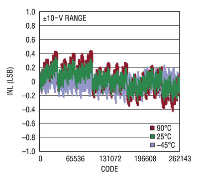
Fig. 2. The LTC2757 18-bit DAC offers ±1-LSB mMax INL and DNL guaranteed from 40 to 85C and settles from a 10-V step to within 1 LSB in 2.0 µs.
The output amplifier used with a current-output R-2R DAC requires not only high open loop gain (>110 dB at 18 bits), but also low offset voltage. The offset voltage is important because any voltage difference between terminals A and B generates a code-dependent error current, which appears as an INL error at the DAC output. The input bias current of the output buffer is less critical, and appears primarily as an offset at the DAC output. Since both amplifier inputs are always at ground, the common-mode rejection of the output amplifier is not critical.
Current-output R-2R DACs that achieve ±1-LSB INL at 16-bits have long been widely available, and a new family of 18-bit DACs from Linear Technology achieves ±4-ppm accuracy, or ±1-LSB max INL at 18-bit resolution, guaranteed over the full temperature range (see Fig. 2 ). The LTC2757 has a parallel interface. The LTC2756 and LTC2758 single and dual 18-bit DACs offer serial SPI interfaces. The LTC2757 INL drift from 40 to 85C is typically less than ±0.2 LSB at 18 bits, and the high 96-dB PSRR renders the output insensitive to supply variation.
Buffered vs. unbuffered
Some high-precision DACs integrate the output amplifier inside the DAC, while others require the use of an external op amp to buffer the output. In both cases, most DACs offer integrated level-shift and feedback resistors to eliminate the need for precision external components.
The primary advantages of integrated output amplifiers are footprint — especially for high-channel-count DACs — and convenience. However an integrated output amplifier may compromise design flexibility.
The combination of output swing, speed, noise, and power offered by the internal amplifier is unlikely to be optimal for a wide range of applications. For example, an integrated single-supply output amplifier will suffer heavily degraded output accuracy near the single-supply rails, so that designers are required to generate a level-shifted differential reference in order to use the full range of DAC output codes. If the negative feedback input of an internal amplifier is not available, designers cannot compensate the output loop to drive large capacitive loads or add an external buffer without a second feedback loop. Users requiring a wider output swing or higher load current will suffer the accuracy, noise, and power penalty of an additional external amplifier stage with an independent feedback loop in series with the internal amplifier loop.
Highest performance is achieved using an unbuffered DAC with an external output amplifier. The wide range of available components gives designers the freedom to choose an amplifier circuit with optimum precision, speed, noise, and power for a given application. ■
Advertisement
Learn more about Linear Technology


