Quantum-dot-based material may revolutionize imagers
In late March, InVisage Technologies, a three-and-a-half-year-old Silicon Valley startup, announced it had developed a new material it says will significantly increase the light-gathering efficiency of imagers, thereby doubling their dynamic range and quadrupling their performance in comparison to today’s chips. The material, called QuantumFilm, is the first to employ quantum-dot technology to benefit imager performance.
“It is becoming increasingly difficult and expensive to develop next-generation image sensors using silicon; essentially, silicon has hit a wall,” claims InVisage President and CEO Jess Lee. “The fundamental problem is that silicon cannot capture light efficiently, but until now it has been the only option.” The current crop of silicon-based image sensors used in such things as mobile phones and security and automotive cameras only capture about 25% of the light that impinges on them. QuantumFilm, on the other hand, captures between 90 and 95% of the light, enabling better pictures even under extremely high-speed or low lighting conditions.
The quantum-dot material was developed under the guidance of Chief Technical Officer Ted Sargent, who is also a professor at the University of Toronto, a visit professor of Nanotechnology at MIT, one of the Scientific American 50, and was dubbed “one of the world’s top young innovators” by MIT’s Technology Review Magazine. Working with VP of Engineering Mike Brading, who previously led Micron Technology’s CMOS SoC sensor design team, and VP of R&D Igor Ivanov, who founded Blue 29 to drive new copper metallization processes, Sargent spent three years engineering the material to produce highly-sensitive image sensors that integrate with standard CMOS manufacturing processes.
QuantumFilm material is deposited directly on top of the wafer during manufacturing (see fig. ). Unlike silicon-based image sensor technologies such as BSI (back-side illumination) and FSI (front-side illumination), the light gathering material covers 100% of each pixel area, capturing all light. Thus it allows more pixels in less area; current QuantumFilm developments are at a 1.1-μm pixel size, versus standard silicon’s low of 1.4 μm.
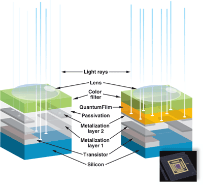
The quantum-dot-based technology developed by InVisage puts the light-gathering process at the top of the chip, thereby preventing the light loss caused by metallization and transistor layers. Use of the material can reduce overall pixel dimensions and the thickness of the silicon, and the process for applying the material fits into existing sensor manufacturing lines. A prototype QuantumFilm device is shown in the inset.
Since the material is added in a final wafer-level process before the addition of the color filter and lens, it can be easily integrated into existing foundries using standard semiconductor processes. Similar to coating a layer of photoresist onto a standard wafer, the QuantumFilm process adds minimal processing cost while eliminating the need for a final passivation coating.
The first QuantumFilm-enabled image sensors, targeting high-end mobile handsets and smart phones, will sample in Q4 of 2010. But QuantumFilm also shows promise for other applications which, in the long run, could prove even more lucrative. For instances, the material’s light capturing capability could be put to use in solar cells, thereby increasing their efficiency. And the quantum-dot technology could also be used to generate light, thus creating new high-pixel, high-resolution displays. (For more information visit http://www.invisageinc.com, call 408-916-5572, or e-mail contactus@invisageinc.com.)
Richard Comerford
Advertisement
Learn more about InVisage


