Testing high-performance mixed-signal designs
In today’s digital systems, ensuring that all elements are synchronized and act as an integrated whole is a major challenge
BY CHRIS LOBERG
Tektronix, Beaverton, OR
http://www.tektronix.com
Embedded and computing systems have become increasingly more powerful by incorporating high-speed buses, industry standard subsystems, and more high-integrated-functionality chips. They have also become more complex, more sensitive to signal quality, and more time consuming to troubleshoot.
While standards exist for many technologies commonly used within high-performance digital systems, a major test challenge is to ensure that these elements are synchronized and perform as a seamless, integrated whole. When hardware and software engineers are working together to troubleshoot the root cause of a specific problem, they require a complete view of information on a bus both its electrical representation and a higher level of abstraction like the decoded view of a serial bus protocol. Testing, debugging, and validating a more-complex high-performance design, typically with multiple subsystems, requires the ability to time-correlate analog and digital signal information.
In such scenarios, engineers are turning to high-performance mixed-signal oscilloscopes (MSOs) that can provide accurate information on timing performance along with views for analyzing data at higher levels of abstraction. While MSOs have been available for some time, only recently have they achieved performance levels necessary to allow debugging of the latest high-speed serial memory and RF systems.
Analog-digital correlation
The context surrounding an event, provided by time-correlated analog and digital signal information, can be invaluable in debugging digital systems. For example, what memory location was being accessed? Where did this packet of information originate? What was the state of the ASIC when that bus fault occurred? Low-level or physical layer details can help identify root cause but often the most efficient way to trace issues is to understand in what state was the larger system. Being able to capture several views of signaling as it flows through a system can provide useful clues and insights.
It is often valuable to analyze specific cycle types, such as signal integrity during read cycles or write timing jitter for a specific bank of memory. Sophisticated signaling schemes such as in DDR can complicate debugging. When cycle information is distributed across several digital signals, it takes sophisticated triggering to respond to it in real time. Thus, effective debugging may include detecting signal faults only during specific bus cycles. Digital pattern qualification can be applied to logic-fault trigger types to detect signal faults in real time, such as a glitch during a read.
High-speed serial designs
High-speed serial bus architectures, including PCI-Express, HDMI, and SATA, provide considerable data throughput along with such benefits as differential signaling, lower pin count, and less space for board layout. As multi-gigabit data rates become common, signal integrity is a critical concern. One bad bit in the data stream can impact the outcome of an instruction or transaction.
High-performance video systems, such as high-end set top boxes, incorporate a variety of technologies such as RF receivers, video processors, memory and high-speed serial interfaces. In this case, the system uses an HDMI interface which operates at 3.4 Gb/s across each of the three data lanes. The architecture of the HDMI link (see Fig. 1 ) includes high-speed clock and data lines, along with the display data channel (DDC), which uses I2 C signaling in standard mode (10 MHz). The DDC line is used for information exchange between the source (transmitter) and sink (receiver) devices.
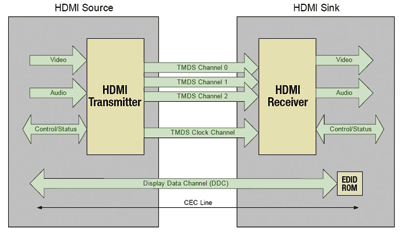
Fig. 1. The HDMI system architecture includes high-speed clock and data lines along with the display data channel.
This design required debug as the output to the monitor would turn off intermittently. First the physical layer was checked for functional operation and each lane passed eye diagram and jitter measurements. After the high-speed clock and data lines were measured, the I2 C control lines were monitored for error codes or invalid data. In normal operation the DDC uses addresses 0xA0 and 0xA1. Using an MSO, engineering were able to capture and decode the I2 C traffic and discover that an incorrect address would sometimes be asserted during power up. In the display of the SDATA line in digital and analog format (see Fig. 2 ), it appeared, based on the analog signal view, that there was crosstalk or other noise-coupling effects that corrupted the I2 C traffic.
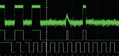
Fig. 2. A display of the SDATA line in digital and analog format makes clear the glitch on I2 C SDATA line was due to noise-coupling effects.
In order to find the root cause of the glitch, adjacent lanes were analyzed and edge rates were evaluated across each high-speed lane. Figure 3 shows a 19-µs time window with a trend plot of edges occurring close to the glitch (see Fig. 3 ), provides some insight into what caused the signal anomaly. The minimum measured rise time of 53 ps was much faster than the 90 to 100 ps edge rates typically found in HDMI systems. The design was then modified to slow the edge rates and the data and clock shielding lines were also improved.
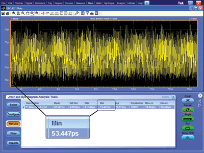
Fig. 3. In this trend plot of rise times within a 19-μs window near the I2 C glitch, the fastest edge rate measured is about 53 ps.
RF test
One of the challenges with software defined radio design is troubleshooting and mitigation of hardware and software errors. As DSP controls more and more of the analog functionality, illegal state or filter values in the digital baseband portion of a design can manifest themselves as RF spectrum errors when they are propagated to the filtering and amplifier portions of a transmitter.
Time correlated analog and digital views facilitate the task of complex multi-domain analysis. Aided by vector signal analysis software, a thorough analysis that includes the frequency-, time-, and modulation- domains can be performed on the same data acquisition. To illustrate this, an MSO’s logic trigger was set to catch an illegal state value to the input of a DAC in a transmitter design. The logic trigger for an all “1” state value (0x3F) triggers the acquisition. The correlated view of the analog signal (see Fig. 4 ) is shown delayed in time by about 34 ns. This represented the absolute delay in the DAC conversion process of this high-speed device.
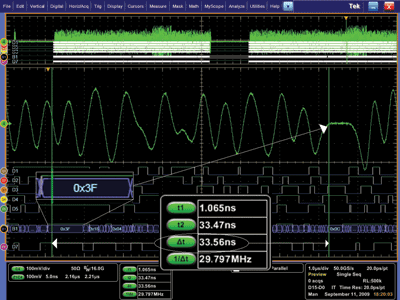
Fig. 4. This integrated view shows the logic states at the DAC and analog output.
This analysis enabled the mulit-domain correlated analysis of a signal to the logic state to the spectral regrowth appearing within a pulsed signal on an analog channel. The time domain view of the RF signal did not provide the complete view of the impact this might have on a software radio design, so further correlated analysis of the RF performance was required.
To assess the RF performance of the signal on the same acquisition, software analysis was performed on the same data set (see Fig. 5 ). A logic state trigger was used to trigger the data set and discrete Fourier transforms (DFTs) were performed to show the Spectrogram and Spectrum frequency domain analysis, and time sampled data is displayed as RF I&Q vs. time and amplitude vs. time.
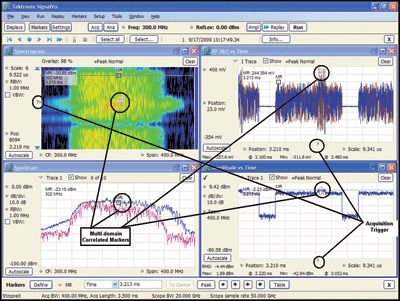
Fig. 5. Time correlated multi-domain views allow in-depth analysis.
Time correlated markers were turned on to demonstrate the time-correlation of the RF analysis for different views. This revealed that the illegal state values triggered at the DAC resulted in a spectral regrowth at RF. The RF regrowth can be traced back to the digital state in the block diagram, thus ruling out a hardware problem in the analog portion of the transmitter. ■
Advertisement
Learn more about Tektronix


