Here are some of the design methods employed in pairing high-speed digital switch fabric with analog SerDes
BY TREVOR HIATT
IDT, San Jose, CA
http://idt.com
The Serial RapidIO Gen2 specification includes significant enhancements to the physical, logical, and transaction layers. The physical-layer spec has doubled the per-lane performance to 6.25 Gbaud and doubled the target transmission distance to 100 cm of FR4 and two connectors, while simultaneously reducing the bit error rate (BER) by three orders of magnitude (to 10–15 ).
This article details some of the design methods employed in developing a 240-Gbit/s Gen2 digital switch fabric along with analog SerDes and high-speed packaging to meet the stringent, high-performance Serial RapidIO Gen2 specification, while ensuring the high-speed analog does not impact the high-performance digital core (or the converse) of the Gen2 devices. The article also explains some of the resultant usage implications in moving to Serial RapidIO Gen2 SerDes performance.
Physical-layer enhancements
The Gen2 physical-layer specification includes new port lane widths of 2x, 8x, and 16x to complement the 1x and 4x from the Gen1 specification. Many endpoint and switch devices that have entered the market support 4x, 2x, and 1x ports for up to 20 Gbits/s of raw throughput, which more than doubles the capacity of 10 Gigabit Ethernet solutions and surpasses PCI Express Gen2 by 25%.
The Serial RapidIO Gen2 specification covers all the classical electrical specifications for short-, medium- and long-reach transmitters and receivers, including eye masks where appropriate. The Gen1 specification did not require equalization of any kind, and some vendors elected optionally to implement equalization. However, the Gen2 specification requires equalization at 6.25 Gbaud for all reaches. At 5 Gbaud, it will likely be needed for long reach, and is optional for short and medium reach. At 6.25-Gbaud long reach, there is no receiver eye mask specified because there may be no eye at the end of the channel. This has clear implications to what the user in the lab may do to determine the signal integrity seen at the receiving device.
SerDes pattern generation and checking (for example, transmitting a pseudo-random bit sequence (PRBS) pattern and checking it at the receiver) is not required in the Serial RapidIO specification, though some device vendors employ these proprietary feature sets. One BER characterization feature new in the Serial RapidIO Gen2 is the per-lane 8b/10b decode error counters. While multiple bit errors in a given code group may not be counted, errors at this level would likely indicate a heavily degraded line. Instead, this counter provides a very good indication of the true BER for reasonably healthy lines with a BER of approximately 10-9 or better.
SerDes: equalization, on-die scope, BER testing
IDT, the leading supplier of Serial RapidIO switches, recently announced the availability of CPS-1848 and CPS-1616 Gen2 switches. To meet the stringent Serial RapidIO Gen2 specification characteristics, IDT designed a 6.25-Gbaud receiver that employs Continuous time equalization (CTE) and decision feedback equalization (DFE).
CTE provides a single zero to boost amplification of the frequency of interest for example, half the baud rate). This is an active amplification, but is performed in a passive fashion on all received bits. This boost on a given band improves the gain of the received signal, while minimizing noise gain.
A five-tap DFE was also employed. DFE provides very selective gain while simultaneously minimizing noise when boosting signals. DFE is used to compensate for inter symbol interference (ISI) — the negative impact to each new bit by the previously transmitted bits. DFE actively looks at the previous transmitted bit history (in this case, up to four previous bits) and feeds back a decision based on this history on how to boost each bit. In this manner, the receiver can remove the ISI frequency effect that would otherwise interfere with the next incoming signal.
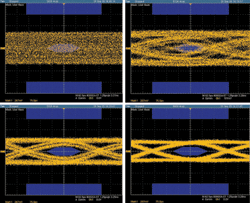
Fig. 1. Classic depiction of the impact of controlling drive strength and pre-emphasis on the signal received at the end of a backplane. Baseline is upper left. Increase of drive strength and 20% pre-emphasis is upper right. 30% pre-emphasis is bottom left. 40% pre-emphasis is bottom right.
A variety of design implementations and features were developed to minimize power. For example, the transmitter provides a great degree of swing control (drive strength and pre-emphasis). The user does not have to stick with what’s required in the standard at the expense of BER. At the receiver, a half rate clock provides significant power savings. This architecture splits the receive data path into even and odd bits, and then leverages a clock running at half the clock speed.
Notably, the DFE circuitry was also architected to support this split data path and half clock rate architecture. Regarding DFE, features to minimize power include allowing the user to turn off unused taps.
To minimize noise on the SerDes, decoupling caps were used to fill in all available silicon space to reduce the noise from the digital logic. Also, differential clock distribution was used for the reference clock to all the device’s PLLs, as well as from the circuitry of those PLLs at each lane. The differential clock distribution improves the clock’s noise immunity. Additionally, the SerDes was isolated by physical distance from the digital core, minimizing digital switching noise on the analog circuitry.
Ensuring a proper high-speed signal
At 6.25 Gbaud, the channel engineering and design is ever more critical and coupled to the transceiver. Indeed, at this rate, the Serial RapidIO Gen2 specification defers to StatEye-compliant transceivers and channels. One can design a StatEye-compliant transceiver against a StatEye-compliant channel model and/or one can design a StatEye-compliant channel against a StatEye-compliant transceiver model. The channel and transceiver are inseparable in complying with specifications.
This has ramifications all the way down to the package design. IDT designed the switches’ flip-chip ball-grid-array (FCBGA) packages to meet specification requirements — the package itself is a part of the channel and its design was performed in coordination with the chip itself, with internal BGA trace lengths minimized, lane pairs carefully matched, and characteristic impedance achieved.
To help ensure transmitted signals do not couple into receiver lanes, the CPS-1848 has ground supply isolation pins between Tx and Rx pins (see Fig. 2 ). Further, power supply pins divide each lane to reduce coupling from one lane into the next. Power-ground loop inductance is minimized by providing core Vdd and ground in a checkerboard fashion. This allows easy application of decoupling capacitors to the PCB’s secondary side.
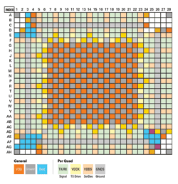
Fig. 2. In a CPS-1848 pPinout, . pPins are color coded. C and checkerboard core and Tx and Rx isolation can be identified.
To improve signaling for the high-speed Serial RapidIO lines, via anti-pads are used to clear the signal via pad from the ground plane on the same layer as the pad. To remove excess capacitance, the anti-pad clearance for the laser via pad is increased from 50 to 100 µm and for the core via pad from 100 to 150 µm (see Fig. 3 ). This can have an impact by improving return loss by 12.5 dB at 5.0 GHz, for example.

Fig. 3. Before (left) and after (right) via hole widening.
To minimize noise from the digital core into the high-speed SerDes and PLLs, the device and package provide separate core and analog supply rails. The device data sheet requires the PCB designer keep these separate. A dedicated SerDes transmitter supply (Vddtx) runs at 1.2 V, though the device is fabricated on a 1.0-V core process. This 1.2-V supply ensures strong transmit swing to guarantee Serial RapidIO transmitter specifications are met with margin.
Usage considerations
As mentioned before, over long reach at 6.25 Gbaud, there may be no eye to scope at the receiver. At these lane rates, oscilloscopes costing $100,000 or more would typically be required to review the signal integrity.
Further, receiver equalization can improve the signal seen at the receiver. Truly, what an oscilloscope sees external to the device may be much worse than what is seen by the actual die, post-equalization. With receiver equalization, On-Die Scope becomes a very useful tool to see what the device sees.
The IDT Gen2 switches all employ a per-lane On-Die Scope that is pattern agnostic. This may be used against any arbitrary pattern, including PRBS-31 test patterns as specified in the Serial RapidIO specification, as well as the Serial RapidIO run-time protocol while packets are traversing the links. On-Die Scope is great for quickly roughing in best transmitter and receiver settings, including equalization settings by simply watching for best eye opening.
A PRBS-31 test pattern may be an ideal and stringent way to characterize the channel, but it has a broader bit transition spectrum than would be seen under a standard Serial RapidIO protocol during run-time. As mentioned previously, PRBS pattern generators and checkers are not required in the Serial RapidIO specification. Run-time BER in the Serial RapidIO system will be lower than what would be seen by the PRBS pattern. Determining the run-time system BER is arguably better served by using Serial RapidIO Gen2’s 8b/10b decode error counters. ■
Advertisement
Learn more about Integrated Device Technology (IDT)


