Devices could be made using a less pure, and therefore less expensive, silicon that would be purified during manufacture
Most materials melt — transition from a solid state to a liquid state — as they get warmer. Only a few materials do the reverse — they melt as they get cooler. Recently, researchers from MIT (Cambridge, MA) discovered that silicon can exhibit such “retrograde melting” when it contains high concentration of certain metals dissolved in it. The findings could someday be useful in lowering manufacturing costs for some silicon-based devices, especially those in which tiny amounts of impurities can significantly reduce performance.

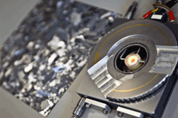
A tiny silicon chip — the orange square at the center of this heating device — is heated to a temperature well below silicon’s melting point, and then very slowly cooled down. The chip inside this heating device was placed in the path of a synchrotron beam to probe its changes at a molecular level as it went through the retrograde melting process. (Photo: Patrick Gillooly)
A compound of silicon, copper, nickel, and iron, the material studied melts as it cools below 900°C, whereas silicon ordinarily melts at 1,414°C. Having lower temperatures makes it possible to observe the behavior of the material during melting, based on x-ray fluorescence microprobe technology using a synchrotron (a type of particle accelerator) as a source.
The researchers discovered that impurities tend to migrate to the liquid portion, leaving regions of purer silicon behind. This could make it possible someday to produce some silicon-based devices, such as solar cells, using a less pure, and therefore less expensive, grade of silicon that would be purified during the manufacturing process.
According to the team leader, Tonio Buonassisi, the SMA Assistant Professor of Mechanical Engineering and Manufacturing, “If you can create little liquid droplets inside a block of silicon, they serve like little vacuum cleaners to suck up impurities.” This research could also lead to new methods for making arrays of silicon nanowires — tiny tubes that are highly conductive to heat and electricity.
The material and its properties are described in a paper just published online in the journal Advanced Materials. More information can be found on http://web.mit.edu/press/ or by e-mailing the MIT press office at media-team@mit.edu.
Christina Nickolas
Advertisement
Learn more about MIT


