Amplifier and video filter board design tips
What can a designer do to ensure the layout avoids oscillation, distortion, and poor overall signal quality?
BY BILL BOLDT and ALLEN WATKINS
Signal Conditioning Products
Fairchild Semiconductor
www.fairchildsemi.com
IC amplifiers are among the most basic building blocks in any designer’s tool box and represent one of the most versatile products available. An amp can provide a wide variety of functions such as driving ADCs, drive multiple video loads, operate as video or other types of filter, drive high-speed instrumentation signals, and much more.
It can also act as an oscillator, but that can actually be a problem since an amp should oscillate only when the designer wants it to. However, an amp can have a mind of its own and oscillate at will if the board is designed incorrectly.
So what should a designer do to protect against unwanted oscillation? The main thing is to recall the lessons of early electronics classes, which taught that oscillation is a function of capacitance, inductance, and feedback. So, the key is to make sure that any extraneous capacitive and inductive feedback paths are reduced or eliminated by designing the board carefully. This is especially important for higher-speed amps (greater than 50 MHz).
Layout consideration
Invisible sources of capacitance and inductance can come from the board, the load (especially if the load is capacitive), and/or the layout. Also, currents flowing to bypass capacitors on different places on the board can take different paths which can lead to distortion. So, ironically, some techniques for reducing distortion are the opposite of what is recommended to guard against oscillation. Here are some layout considerations to keep in mind to fight distortion and oscillation when designing in an amp or video filter.
Looking first at oscillation, when directly driving a capacitive load with an amp, the load together with amp’s output impedance creates phase lag that can cause peaking or oscillation. Some amps can drive capacitive loads, but for those that cannot, a small series resistance (Rs) placed at the amp’s output can enhance stability and settling time (see Fig. 1 ).
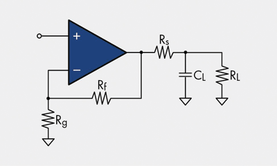
Fig 1: A small series resistance (Rs) at the amplifier’s output can enhance stability and settling time.
When driving a transmission cable with an inherent impedance (such as a coax cable) as shown in Fig. 2 , resistors Rs and RL should be set equal to the cable’s impedance (Zo), and the capacitor C should be set to match the cable impedance over a wide frequency range to compensate for the amp’s increasing output impedance (with increasing frequency).
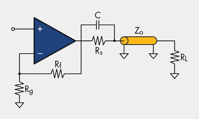
Fig 2: Driving cable or transmission Line
High-frequency amps are subject to layout-induced distortion, yet even lower-frequency amps, such as audio, can have very stringent distortion requirements. Distortion (THD) is a classic measure of audio quality making layout for distortion reduction critical.
An important source of distortion comes from ground current effects in a PCB. The mechanism stems from current flowing to bypass capacitors for each supply voltage and to the supplies being proportional to the conductance present in the path. Different paths can mean different conductance leading to distortion because even though the material of a PCB itself is linear, the board behaves in a “spatially nonlinear” fashion. This is because bypass capacitors are placed at different locations on the board, which leads to ground currents flowing to their respective bypass capacitors along different paths.
The different paths cause a fraction of one polarity of ground current flowing past the input resistor ground to affect the voltage for only that polarity, while the other polarity of ground current can remain unaffected. The result is that the input signal voltage is modified unevenly creating a nonlinear event.
In this case, if one polarity is modified while the other is not, then second-harmonic distortion is created. To state it another way, when only one polarity of a sine wave is modified, the result is no longer a sine wave and the effect from such distortion can be noticeable. To protect against distortion, the designer can use common ground points and ground bypass capacitors on the output side.
The cardinal rule in high-frequency board layout is to place the high-frequency bypass capacitors as close to the package supply pins as possible. However, experiments have shown that slight lengthening of the traces to the high-frequency bypass connections can improve distortion performance by improving flatness and differential gain. Rules of thumb are useful but a designer’s experimental side can come in handy to make sure the rules reflect reality.
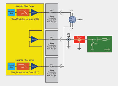
Fig. 3: Shown is the schematic representation of a video filter/driver used in a system as the output driver to a media device.
In order to obtain the highest quality output signal the series termination resistor must be placed as close to the device output pin as possible. This will greatly reduce the parasitic capacitance and inductance effect on the output of the driver. The distance from device pin to place series termination resistor should be no greater than 0.5 in.
Figure 3 is the schematic representation of a video filter/driver used in a system as the output driver to a media device. Here the composite video signal is terminated by the media device and the S-video output terminations are open. It is very critical in this case to have the series termination resistors close to the output pin of the device to minimize the effects of parasitic capacitance on the filter output driver, which may show up as oscillations on the output.
Figure 4 compares Fairchild’s FMS6346A video filter driver driving 25- and 47-pF loads. This demonstrates that the performance is better with lower capacitance, and if we try to drive more capacitance than the specified maximum it is very likely that oscillations will occur on the system output.
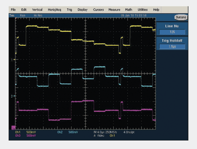
Fig. 4: Comparison of an FMS6346A driving 25- and 47-pF loads.
So, given all the possible effects of layout on performance, what can a designer do to ensure the layout avoids oscillation, distortion, and poor overall signal quality? The “Lucky 13” basic layout and bypassing guidelines can be of assistance:
“Lucky 13”
1. RTM (Read The Manual). A typical data sheet for an amp will call out its minimum stable gain requirements. This is critical since operating an amp at gains below recommended levels can lead to oscillation.
2. Use a ground plane. Ground planes are the best way to provide low induction ground connections.
3. Eliminate ground planes under and around amps and around the sensitive pins. Eliminating the ground plane near the input and output pins of a high-speed amp can reduce unwanted capacitance It is also helpful to keep the ground plane away from under and surrounding a high-speed amp for the same reason.
4. Use surface-mount components. Surface mount components have inherently low lead inductances.
5. Minimize the lead lengths. Keeping leads short reduces series inductances at the inverting input of the amp.
6. Avoid sockets. Avoiding sockets or at least using flush-mount sockets can reduce inductance.
7. Use the recommended feedback resistor value. This is important when using a current-feedback amp.
8. Do not use a nonlinear element (e.g. a capacitor) in the amp’s direct feedback loop.
9. Use a feedback resistor for unity gain configurations. Do not use a standard voltage-follower circuit.
10. Use bypass capacitors. Bypass capacitors on each supply can provide a low impedance return current path to the power pins, improve power supply noise rejection, and provide high-frequency filtering on the power supply traces. Most manufacturers recommend 6.8-µF tantalum capacitors and 0.1-µF ceramic capacitors. For optimal performance, place a 6.8-µF capacitor within 0.75 in. of the power pin and the 0.1-µF capacitor within 0.1 in. of the power pin. As the distance increases, capacitors become less effective due to added trace inductance. However, the distance needs to be balanced with distortion considerations since experiments show that a little bit of lengthening of the distance can improve distortion performance.
11. Try rotating or rearranging bypass capacitors to reduce distortion. When single op amps display distortion induced by ground current paths, the ground current flow can be adjusted and kept away from the input components by rearranging the bypass elements. This can be as simple as rotating a bypass capacitor to move its ground connection away from the inputs.
12. For video filters keep series termination resistors close to the output pin. This will minimize the effects of parasitic capacitance on the filter output driver which may show up as oscillations on the output.
13. Place the input coupling capacitor and termination resistor close to the input pin for optimal signal integrity.
Board layout plays a crucial role in system performance and should be carefully monitored during the design and layout phase. When in doubt, call your amp or video filter supplier. They will be happy to help. ■
Advertisement
Learn more about Fairchild Semiconductor


