Optimized IGBTs support specialized application requirements
BY MARK THOMAS and THOMAS KIMMER
Infineon Technologies, Villach, Austria
www.infineon.com
Evolutionary improvement in production and packaging of the IGBT (insulated-gate bipolar transistor) is broadening the range of applications served by this workhorse power-switching technology. The basic concept of the IGBT is to act as a switching device with bipolar action (high current density) and a high-impedance gate as found on a MOSFET device. Although IGBTs were conceived in the late 1960s, it took until the mid-1980s for commercially viable devices to be available.
The first IGBTs using the “punchthrough” (PT) concept could switch up to 15 kHz, but the negative temperature coefficient of VCE(sat) created a high risk of thermal runaway when paralleling the devices. Cost improvements based on the use of homogenous raw materials and process innovation led to “non-punch-through” (NPT) IGBTs in 1999. These supported switching frequencies up to 30 kHz and had a positive temperature coefficient of VCE(sat) , meaning paralleling of devices was easier. The longer channel of the vertical structure, however, resulted in a higher VCE(sat) value, so conduction losses increased.
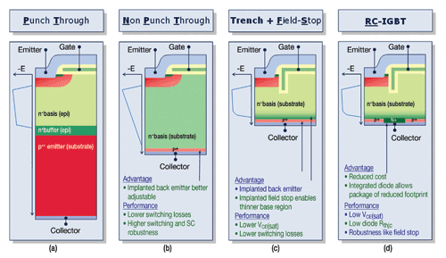
Fig. 1: The evolution of IGBT technology.
Field-stop and Infineon-patented TrenchStop concepts were introduced in 2002 (as 1,200-V devices, followed by 600-V devices in 2003). The vertical trench structure of the gate enabled higher current density, and the field-stop implant allows wafer thinning that gives a shorter tail current during switch-off. The thinner wafer and resultant shorter channel provided the triple-win situation of approximately 40% reduction in the conduction losses with no penalty against switching losses plus 10% reduction in production costs (Fig. 1c ) compared to earlier devices.
Fine-tuning the process technology has been the focus of IGBT manufacturers throughout this decade. Infineon’s High Speed 3 generation IGBT family (2010 production) supports applications switching up to 100 kHz with turn-off losses 35% lower than the previous generation of NPT IGBTs. With lower production cost, the sample pricing of devices in this family ranges from EUR 1.90 (600 V, 20 A) to EUR 5.10 (1,200 V, 40 A).
Application-optimized IGBTs
Increased efficiency and improved system cost remain mantras for both traditional IGBT applications — such as photovoltaic inverter, UPS, and welding systems — and newer segments like electric/hybrid vehicles, induction cook tops, and switch-mode power supplies.
For example, integration of the free-wheeling diode into the IGBT cell design (Fig. 1d ) led to new reverse conducting devices (RC-IGBTs). With reduced total system silicon cost, these are ideal for applications such as induction cooking.
Automotive applications are another growth area for IGBTs. Discrete devices that have an inherent junction temperature up to 175°C are part of inverter designs in some EVs available today, such as Tesla. Future advances in packaging and continued cost improvement will see module designs that simplify adoption in both HEV and EV cars.
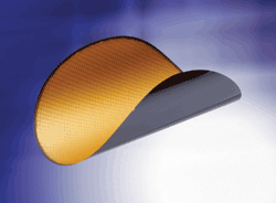
Fig. 2: Reduction of wafer thickness, to 40 µm as seen here, provides low-saturation-voltage IGBTs.
Further advances in thin-wafer TrenchStop IGBTs are likely to include new IGBT cell structures for increased current density, reduction in wafer thickness below 40 µm, advances in base raw material, and packaging improvement (see Fig. 2 ). So while the high-efficiency power-switch market will expand to include GaN and SiC JFETs, the IGBT will remain popular as a cost-effective, high-efficiency device that can be customized for individual applications. ■
Advertisement
Learn more about Infineon Technologies


