Debugging common digital problems with a scope
As system speeds increase and designs shrink, circuit designers increasingly must debug signal integrity problems
BY GINA BONINI
Worldwide Embedded-Systems
Technical-marketing Manager
Tektronix
www.tek.com
Embedded systems can contain many different types of devices including microcontrollers, microprocessors, DSPs, RAM, EPROMs, FPGAs, A/Ds, and D/As. These various devices must communicate with each other and the outside world using data buses. However, as system speeds increase and designs shrink, circuit designers increasingly must debug signal integrity problems.
The ideal digital signal has fast transitions and only two states: high and low. In the real world, digital signals are much more complex (see Fig. 1 ). The deviations from ideal are known as signal integrity issues. Since these problems can result in incorrect data patterns affecting system operation, designers commonly must analyze their design’s signal integrity to ensure proper operation.
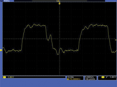
Fig. 1: Digital signals are interpreted by a system as high and low states, above and below a defined voltage threshold. In practice, especially at higher speeds, digital signals are rarely ideal with flat high and low levels and clean edge transitions.
There are two fundamental sources of signal degradation – timing errors and physical layer issues. Timing errors are caused by what the name implies system or component timing issues. These typically manifest as glitches, runts or wrong logic levels. Physical layer issues often have their origins in circuit-board design or signal termination.
Common timing errors
The most common sources of timing errors are bus contention, setup and hold violations, and metastability. Bus contention occurs when two driver devices try to drive the same bus line at the same time. If the inactive driver doesn’t change to a high-impedance state in time, the two drivers then contend for the bus. Neither driver prevails, forcing the bus to an indeterminate amplitude that may fail to reach the threshold voltage.
With regard to setup and hold violations, consider that a clocked device requires the data to be stable at its input for a specified time before the clock arrives. This is known as “setup” time. Similarly, the input data must remain valid for a specified time after the clock edge. This is known as “hold” time. Violating setup and/or hold requirements can cause unpredictable glitches on the output.
Metastability is an indeterminate or unstable data state on the output of a logic device that results from a timing violation, such as a setup and hold problem. As a result, the output signal might be late or achieve an illegal output level, such as a runt, a glitch, or even the wrong logic level.
Common PHY layer issues
The most common issues with regard to the physical layer are amplitude problems, edge aberrations, reflections, crosstalk, and ground bounce. Amplitude problems include ringing (oscillation), droop (decreased amplitude at the start of a pulse), and runt pulses (those which do not reach full amplitude). There are many potential causes to amplitude problems, including unintended inductance loops, filtering, and signal loss.
Edge aberrations can result from board layout problems or from improper termination or even quality problems in the semiconductor devices. Aberrations can include preshoot, rounding, overshoot, ringing, nonmonotonic edges, and slow rise time.
Reflections can be caused by termination and board layout problems, where the outgoing signal bounces back toward its source and interferes with subsequent pulses.
Crosstalk can occur when long traces running next to each other couple their signals together through mutual capacitance and inductance. In addition, the higher current embodied in fast edges increases the amount of radiated magnetic energy, and with it, crosstalk.
Ground bounce, caused by excessive current draw (and/or resistance in the power supply and ground return paths), can cause a circuit’s ground reference level to shift when current demands are high.
Debugging signal integrity problems
Validating and debugging complex embedded systems requires analyzing digital signals, often in both the digital domain and analog domain, to look for common signal integrity issues. With modern mixed signal oscilloscopes (MSOs), one instrument can be used for all these tasks. An MSO lets an engineer look at their signals in both the digital domain using the digital channels, and analog domain using the traditional oscilloscope analog channels (see Fig. 2 ).
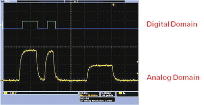
Fig. 2: In the digital domain, the digital signal appears to be behaving correctly. In the analog domain, there is clear evidence of a runt and negative glitch (or dropout) indicating problems in the design.
In the digital domain, the oscilloscope displays the signal as a logic circuit would interpret it. The oscilloscope compares the incoming signal to a logic threshold; if the signal is above the threshold, the oscilloscope displays a logic high. Otherwise, a logic low is displayed.
Some MSOs will allow the engineer to define one signal as a clock. The clock will then be used to determine when the oscilloscope samples the other digital signals. In this mode, the resulting display is called a state diagram. If no clock is defined, then the oscilloscope will sample based on the digital sample rate of the channel, and in this mode the resulting display is called a timing diagram.
The digital domain is useful in determining if signal integrity problems will affect the design’s operation. As long as ringing, overshoot, ground bounce, and such do not cause logic transitions, these signal integrity issues should not affect how the device interprets the digital signal.
If an unintended logic transition does occur, the next step in debugging is to take a closer look at the analog domain.
In the analog domain
Many digital problems are much easier to pinpoint if an engineer can see the analog representation of the flawed digital signal. On the analog channels of an oscilloscope, the incoming signal is sampled by the oscilloscope’s ADC. The sample points are then displayed on the oscilloscope screen using sin(x)/x interpolation to reconstruct the analog waveform. This allows the engineer to see how voltage changes over time on their signal. With this view, root cause for problems in the digital domain are often clearer.
In this example, the MSO’s digital channels D0 and D1 are connected to two digital signals. The MSO threshold setting for each channel is set to 2.0 V, the common threshold level for 3.3-V LVPECL logic. A pulse width trigger is set to look for any nonconforming pulses.
As shown in Fig. 3 , the oscilloscope triggered on a glitch (very narrow pulse) which can be seen on the D0 signal. This glitch is only occurring when the D1 signal’s rising edge is occurring. This is typically an indication that crosstalk is occurring between the two signals.
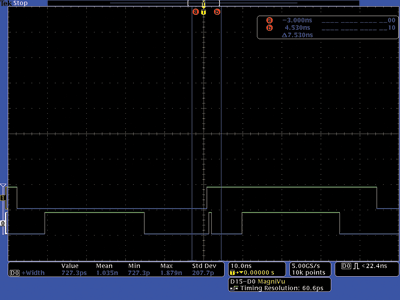
Fig. 3: Notice the glitch on the D0 signal. The glitch appears to only occur when there is a rising edge on the D1 signal.
Next, the digital signals are also connected to the oscilloscope’s analog channels so as to simultaneously show both the analog and digital domain. With this view, spikes can clearly be seen on the adjacent trace when a rising edge occurs on the other trace (see Fig. 4 ). This is a clear indication of crosstalk.
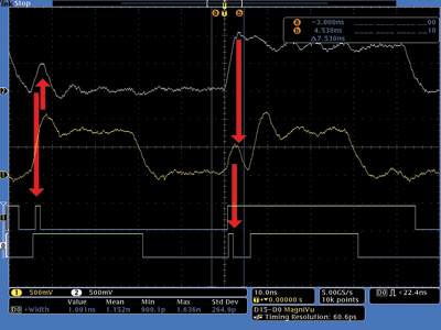
Fig. 4: Notice that a spike occurs in the analog domain on the adjacent trace at each rising edge. This is a clear indication of crosstalk.
Finding and fixingsignal anomalies
As you’ve seen previously there are mainly two types of signal integrity problems that can occur in a digital system: timing and physical layer issues. The first step in fixing these issues is to find and isolate the problem. Is it repeatable? How often? What is the state of the bus when the problem occurred? Most modern oscilloscopes have built-in tools that help designers quickly uncover and capture signal anomalies.
A symptom of common timing problems on data buses, such as bus contention and metastability, is an abnormal digital pulse; a pulse that is too short (runt) or too narrow (glitch) or slow to rise/fall. Physical layer issues may also appear as these signal anomalies.
With an oscilloscope, these problems can be captured by setting up an appropriate trigger (see Fig. 5 ). The oscilloscope will then continuously check the incoming signal looking for a pulse that violates the parameters set. If the oscilloscope triggers, then the engineer knows that an anomaly exists in his signal.
For more elusive problems or to check the stability of a design, the oscilloscope can be set up to monitor the signal for long durations of time throughout the night or over the weekend. Because the oscilloscope constantly monitors the incoming signal, a designer is assured that elusive events will be captured for further analysis.
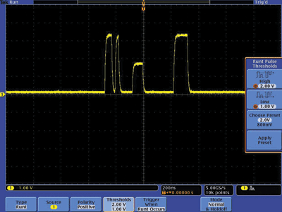
Fig. 5: Using a Runt trigger the small pulse in the middle is easily captured. In this example, 50% of the oscilloscope’s record length is used to capture the signal pretrigger, and 50% after the trigger event occurs.
With the faulty signal captured, the designer can then analyze its characteristics to determine what the root cause of the problem is. It’s helpful for a designer to be able to view signals before and after the trigger event to better understand the context in which the event of interest occurs, or to capture many events of interest for further analysis. ■
Advertisement
Learn more about Tektronix


