Three factors determine the charging IC architecture for a specific design: battery capacity, charge cycle times, and form factor
BY GEORGE PAPARRIZOS
Summit Microelectronics
www.summitmicro.com
This is the second of a multipart series on the fundamentals of battery charging. You can find Part 1 at: www2.electronicproducts.com/Fundamentals_of_battery_charging_Part_1-article-fapo_Summit_may2011-html.aspx
One major distinction among the various battery charging IC solutions is the power architecture they use. Like other power ICs, battery chargers can deliver power either in a linear-mode (think of a linear regulator or LDO) or in a switch-mode (think of a step-down switching regulator). Pulse chargers were also available as of a few years ago, however they have been avoided in modern designs because of their negative effect on battery reliability. While in the past linear charging solutions used to dominate the marketplace because of their low cost and simplified design, the trend for higher processing power and batteries with higher capacity in smartphones and tablets have resulted in the need for more efficient implementations.
Main factors
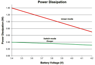
Three main factors will determine the charging IC architecture to be used for a specific design: a) the selected battery capacity, b) the target charge cycle times and c) the industrial design (i.e. form factor) of the portable device. For small battery capacities, a linear-mode charging solution is ideal because of low cost and complexity. As the required charge current levels increase, a switch-mode topology becomes inevitable. The significantly higher efficiency of a switch-mode battery charger IC allows for higher charge current levels (that is, shorter charging times), and at the same time minimizes hot spots — a key issue in modern, compact designs. A switch-mode charger IC is also more desirable in systems that use unregulated or simply higher-voltage wall-adapters, since their power dissipation is not a direct function of input (adapter) to output (battery) voltage differential (see Fig. 4 ). New linear charger IC offerings do incorporate current foldback, which allows the charge current to be reduced as the charger IC die temperature increases, thereby protecting the IC itself. The downside of this operational mode is longer charging times which are the result of the thermally-reduced charge current.

Fig. 4: Example of power dissipation between a linear and a switch-mode charger IC.
There is a variety of charging topologies to choose from based on the system requirements. For example, available charging solutions can support one or two power inputs. If the portable device plans to have only one connector for input power, the charging IC requires only a single input power path (see Fig. 5 ). On the other hand, a lot of handheld equipment support two power inputs; for example, a USB input for universal charging and a barrel input for wall adapter (high-current) charging. In this case the charging IC needs to support two input power paths and to be able to arbitrate between them based on input presence and/or input power priority.
In addition, battery charging devices offer two different output power configurations. The first one provides a single output path for battery charging and system power (see Fig. 5). Such an implementation is simpler and therefore generally lower-cost. In this case the power delivered from the wall adapter, or any other power source (USB hub, solar cell, etc.), is limited by the charger configuration for both the battery and the system. For example, if the input power source provides 5 V and 1 A, the voltage that is delivered to the battery/system node depends on the charging phase (pre-, fast- or taper-charging: 2.8 to 4.2 V) and the current delivered to the battery/system node also depends on the maximum current allowable by the battery pack (for that specific charging phase). Hence, the system does not take advantage of the full power available at the input and some system losses are introduced into the design. Furthermore, in this configuration the battery charger IC cannot differentiate between the current going into the battery and the current going into the system. With this charging architecture, it is also very common that the removal of the battery is considered a fault condition and no power is available to the system. This charging implementation however allows for a simple, low-cost design, and is therefore very popular in consumer electronics.

Fig. 5: Typical charging solutions with one input and one output
Battery-charging solutions with CurrentPath technology provide separate outputs for system and battery power (Fig. 6), that is, they feature two output power paths. In this case, the power delivered from the wall adapter or other power source (USB hub, solar cell, etc.) to the battery is limited by the charger configuration, however the system is directly powered by the input power source. This implementation is more complicated because of the additional power steering paths, however it provides several benefits to both system operation and battery charging/control.
With CurrentPath, when the system is connected directly to the external input power source, the priority for power delivery is the system. This power architecture also enables applications to fully operate even when the battery is not present or deeply discharged, assuming of course that they are connected to the wall adapter. This is a key requirement for many new portable designs, since they support operation without the battery and expect instant system power-up.

Fig. 6: Typical charging solution with one input and two outputs.
Another benefit of separating the path between the battery and the system is the fact that, when the battery is in the pre-charge (pre-conditioning) state and charge current is limited to a 0.1-C level (not sufficient to power-up the system), the power to the system is not compromised because of the independent path. Last but not least, the implementation shown in Figure 6 allows the battery to supplement power to the system, when the system requires more power than what is available from the power source (input source). Figure 6 describes the basic CurrentPath operation under three different conditions. ■
Advertisement
Learn more about Summit Microelectronics


