Power printed circuit board design — boost and buck
Here’s help to gauge trace widths and design layer transitions for high-power, high-yield mass production environments
BY NICHOLAUS W. SMITH
Integrated Device Technology
San Jose, CA
www.idt.com
This paper will provide an overview of the most important aspects of the layout of boost step-up switching regulators and buck step-down switching regulators. There are many similarities in the key features of the layout and component selection of the two regulator types that can result in many percentage points of efficiency loss. This paper will help readers gauge necessary trace widths and design layer transitions for high-power, high-yield mass production environments.
One of the ongoing challenges in the precision analog engineering arena is improving power management efficiencies while increasing analog and digital integrations. As interest grows in power management ICs, it’s become clear to many engineers that there are many similarities between a boost step-up switching regulator and a buck step-down switching regulator. There are multiple factors involved in getting the best performance from a converter, some of which include selecting the proper components to support the IC function and designing the printed circuit board for optimal performance and efficiency. It’s obvious that the layouts of each should be as small and compact as possible but what portion of the design should be first for getting the closest and which one should be compromised due to the physical limitations of the components and the printed circuit board design. Each type of regulator needs to have an input capacitor, an output capacitor and an inductor. Though these guidelines are well known, the reasons behind them are often misunderstood. This paper will explain those reasons, the knowledge of which will ultimately help engineers generate optimal layouts while accepting minimal and reasonable trade-offs.
Inductor selection
This article will address regulators running at fairly high output currents in pulse width modulation (PWM) mode at a fixed frequency; it will assume they do not need to be switched at 100% duty cycle to supply the load. The paper will ignore specifics such as input currents limits, output short-circuit protection, and other design features that enhance product lifetime such as thermal protection. The paper will touch on ac current paths, dc current paths, and routing optimization for highest-efficiency operation. After explaining the routing techniques and reasons behind the placement and routing precedence, the paper will discuss the differences and show how the two layouts are different. This should help engineers to create higher-efficiency regulators.
For the typical switching regulator, there is an input capacitor that will be on the order of 10 to 22 µF, an output capacitor typically in the same farad range, and an inductor that will vary in inductance proportional to output capacitance and switch frequency. Higher switching frequencies allow for inductors with fewer henries of inductance, thus shrinking the inductor but increasing the demand on maintaining small-geometry layouts. When choosing the inductor for the regulator, factors to consider include saturation current, temperature response, space restrictions, and the recommended inductance at room temperature. Normal cases will require an inductor with a 30% saturation current rating when operated at twice the expected dc load current. Lowering the error percentage or increasing the saturation current are ways to improve efficiency beyond the bare minimum but usually come at the cost of board real estate.
Another key factor in inductor selection is to know the self-resonant frequency of the inductor, then solve for the necessary output capacitance to keep the output filter resonant frequency at a minimum of 10 lower than the inductor’s self-resonant frequency. The self-resonant frequency is a value often found on inductor datasheets and included in the model provided by the vendor. Inductance varies with inductor current and temperature, while the coil-to-coil capacitance, the cause of self-resonance, varies with inductor voltage, frequency, and temperature. This may sound a lot like an endless cycle of variation, so this paper will assume the system has stabilized and is operating in steady state. Below are formulas to consider when thinking about inductor selection. This paper assumes the designer has selected an adequate inductor value to match the regulator design and the buck or boost manufacturer has listed this value in its datasheet.
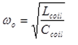
Eq. 1: Coil self-resonant frequency
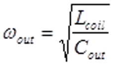
Eq. 2: Regulator resonant frequency
Capacitor selection
The capacitor should be one with a dielectric type that has a minimum temperature rating equal to the IC-specified ambient operating temperature minimum and maximum. Also, the voltage rating should be 1.5 times (or more) the anticipated voltage on the node. The benefit of extra temperature and higher voltage ratings is more stable capacitance for all operating conditions. As the voltage is increased, the capacitance decreases; at the specified voltage, the capacitance is expected to be at its lowest. This is a good value to use to verify that the loop corner frequency is not approaching the inductor’s self-resonant frequency. The best performance is expected to occur at the manufacturer’s recommended values, which means that higher-current-rated inductors and higher-voltage-rated capacitors provide an easy way to get the highest performance out of regulators. The biggest advantage of selecting components with higher temperature specifications is that they provide a more stable capacitance versus temperature, tighter tolerances and lower equivalent series resistances.
Similarities of boost and buck switching regulators
In addition to their input capacitors, output capacitors and inductors, another (occasionally misconstrued) similarity between the two types of integrated regulators is the standard of keeping the components close and the trace lengths short. What is often unknown and easily overlooked if it is not specifically looked for is the reason for the subtle difference in optimal layout between the two regulator types. This difference can result in lower than expected performance and it of course, because of the physics behind the operational difference. These differences must be considered while placing the components.
Buck regulator current paths
As shown in Fig. 1 , at time t1, the current flows from Cin through the input switch to the inductor. From the inductor, the current splits between Cout and the load and recombines while returning to Cin. Then, at time t2, the current comes from Cout and the load return and flows through the IC switch to the inductor. It finally returns to Cout and the load. With these paths in mind, when looking for similarities from time 1 to time 2, the only difference occurs on the left – the addition of the Cin current path and the use of the alternate switch. So, the optimal layout of the buck regulator will have placement and routing emphasis on minimizing the length and maximizing the width of the connections between the input capacitor as well as the IC’s Vin and the PGND pins. Any current flowing in the Cin path when t2 occurs will be lost power returned to te source. The longer the trace, the more energy in the metal, so extra length in this trace will directly influence the overall efficiency.
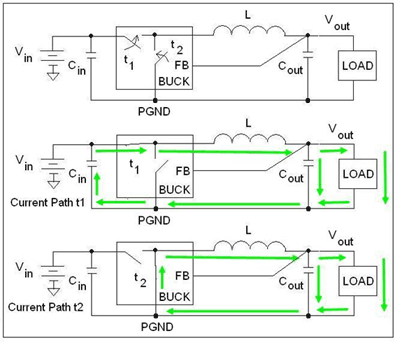
Fig. 1: Buck regulator, inner switches, time 1 current path (t1), time 2 current path (t2)
The next optimization should come by way of placing the GND side of Cout as close as possible to the same PGND connection. Now the inductor should be placed last because the two paths are directly in series with the main inductor. The inductor’s inductance will most likely swamp out any parasitic inductance added by traces, assuming it is placed in close proximity to the IC. The output node should be routed directly from the top of the Cout and FB connection, and the return should route right back to the bottom of the Cout capacitor. Now all the fast-switching AC currents are localized to the DUT and the dc current is properly routed to and from the load. Finally, the PGND node should be tied to the GND symbol. This connection does not have to be too wide, but it should be able to carry the soft start current. Its main purpose is to keep the grounds at the same potential.
Boost regulator current paths
Figure 2 shows the most common boost regulator architecture with the high-current paths highlighted and notated for the two main operating-time-based conditions.

Fig. 2: Boost regulator, inner switches, time 1 current path (t1), time 2 current path (t2)
Looking at the boost figure at times t1 and t2, it should be apparent that again, a section of a current path has stopped being used from one time period to the next. The area of the changing loop area now has to do with the output capacitor and the IC. In this case, placement and layout precedence should be placed first on the Cout capacitor connections to the IC, then the PGND node of the Cin capacitor should be oriented as close as possible to the IC’s PGND pin. Once again, the inductor can be placed last. Next, the feedback node should be tied near the load or at the top of the output capacitor, and the PGND referenced to the input power supply ground. The last technique to optimize the layouts is to keep the area of the changing loops as small as possible since residual currents left behind after switching paths alternate will be lost power. Reducing the loop area usually becomes a three-dimensional problem, so it is best to keep as many traces on the top PCB layer and to route any crossovers on the next closest physical layer to the top layer.
Differences between boost and buck switching regulators
The image in Fig. 3 comes from the IDTP9020 wireless charging IC (due to release in 2012) with an output buck regulator capable of delivering 7.5 W of output power.
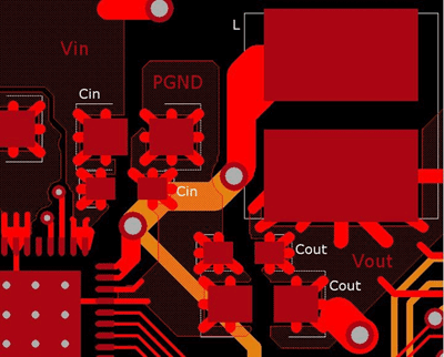
Fig. 3: IDTP9020 buck regulator layout
In this layout image, there are actually two input and two output capacitors. This is done to keep the package sizes and footprint sizes small while increasing the capacitance. The entire changing loop area has been kept on the top layer, with the Cin capacitors kept the closest to the IC and very wide metal used for inter-connections. The wide metal assists in heat dissipation and is low in resistance and inductance. The shaded red areas are solid top metal on the finished circuit board.
The layout in Fig. 4 looks crowded and space-constrained because it is. This device is a complete system-level power management device (among other functions). This paper focuses on a single block of the IC, the Boost5.
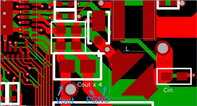
Fig. 4: IDTP95020 Boost5 layout
There are multiple output capacitors (four shown), since this boost was designed for powering an integrated 2.5W class D audio amplifier. These have been placed first and closest to the IC followed by the inductor and the input capacitor in close proximity. In this case, the inductor was placed closer to keep the LX switching node from overlapping with the input capacitor GND return and increases shielding to and from other regulators. Some tradeoffs were made for optimizing the layout of other switching regulators opposed to just this one.
As discussed earlier, it is best to minimize the input capacitor PGND return length and then place the inductor. But, as show here, slight variations are often necessary for the performance of a system. This means that while the ideas presented in this paper are fundamentally sound, there is no one-size-fits-all rule for laying out buck or boost regulators. However, understanding the physical paths used for operation will enable printed circuit board designers to make the right trade-offs to increase regulator efficiency and decrease losses associated with placing priority on the wrong capacitors for the switching regulator type.
Finding the right mix of cost, size, and performance for layout area and component selection is always a challenge, but by using sound engineering guidelines and having a firm understanding of the problem, it becomes less complex to generate optimal layouts while accepting minimal and reasonable trade-offs. ■
Advertisement
Learn more about Integrated Device Technology (IDT)


