Need a microscope? There’s an app for that
Researchers at Michigan Tech develop affordable superlens which could make its way onto future cell phones
A team of Michigan Tech researchers may have found a way to create an ultra-high-resolution microscope that could be used in places as common as the cameras in tomorrow’s smartphones.
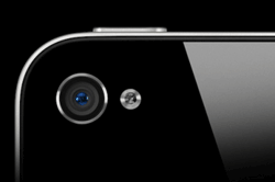
Will a high-resolution microscope be available on your next smartphone? (via: cdn.devicemag.com)
Durdu Guney, an electrical engineer and assistant professor of electrical and computer engineering at Michigan Technological University, believes his team has taken a major step toward creating a superlens (a.k.a. the “perfect lens”) that has the ability to use visible light to see objects 100 nanometers across.
Superlens vs. all other lenses
The best lenses out there won’t let us see objects smaller than 200 nanometers across (about the size of the smallest bacterium). Sure, electron microscopes can let us see objects as small as a nanometer wide, but the problem with them is that they’re huge, heavy, and really expensive.
Enter the superlens.
To build one, you need to use metamaterials; that is, artificial materials with properties not normally found in nature. The material that makes the difference here is plasmons: quasiparticles which result from plasma ocillations near the surface of thin metal films that combine with special nanostructures. When they’re excited by an electromagnetic field, they gather light waves from an object and refract it in a way not seen in nature called negative refraction. This reaction, in turn, allows the lens to overcome its diffraction limit.
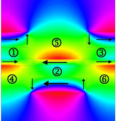
Illustration of Guney’s theoretical metamaterial: Colors show magnetic fields generated by plasmons; black arrows show direction of electrical current in metallic layers, and numbers indicate current loops contributing to negative refraction. (via: mtu.edu)
Overcoming the diffraction limit
While other researchers have sidestepped diffraction limits in the past, what’s particularly noteworthy about Guney’s model is that his covers the ENTIRE spectrum of visible light. That’s because the metamaterials he used are capable of being “stretched,” if you will, to refract light waves from infrared to visible and all the way over to ultraviolet.
Uses
These superlenses are fairly inexpensive to produce. That’s why some are suggesting that they may one day make their way onto cell phones. There are, however, additional uses that Guney pointed out, other than using one’s phone to point out the ridiculous amount of dust mites on a friend’s couch:
“It could also be applied to lithography,” he said, referring to the microfabrication process used in electronics manufacturing. “The lens determines the feature size you can make, and by replacing an old lens with this superlens, you could make smaller features at a lower cost. You could make devices as small as you like.”
Computer chips are a good example. They’re made using UV lasers, which are expensive and difficult to build. With the superlens, all you need is the lens and a red laser, like the pointers that everyone’s used before, to do the same exact job.
Public accessibilty
Guney is particularly excited by what the accessibility of the superlens might do for the general public’s interest in science:
“The public’s access to high-powered microscopes is negligible,” he said. “With superlenses, everybody could be a scientist. People could put their cells on Facebook. It might just inspire society’s scientific soul.”
Published report
Gulney and grad student Muhammad Aslam published an article on their work entitled, “Surface Plasmon Diven Scalable Low-Loss Negative-Index Metamaterial in the visible spectrum.”
It can be found in Physical Review B, volume 84, issue 19.0 . Head to prb.aps.org/abstract/PRB/v84/i19/e195465 to read it for yourself. ■
Reference for this article:
Advertisement
Learn more about Electronic Products Magazine


