Fundamentals: Advanced semiconductor processes
BY BRIAN DIPERT
Principal, Sierra Media
Intel co-founder Gordon Moore first observed (http://en.wikipedia.org/wiki/Moore%27s_law), in a 1965 paper published in Electronics Magazine , that the number of structures integrated on an integrated circuit had doubled every year since the invention of the IC seven years earlier (in 1958). He predicted that this trend would continue “for at least ten years.” Nearly 50 years after that prognostication, and more than 50 years after the IC's first formulation, the pattern has remained unerringly consistent (see Fig. 1 ). And it translates not only into increasingly complex degrees of single-die integration capability, but also to higher switching speeds and lower power consumption befitting the transistors' more compact dimensions and lower operating voltages.
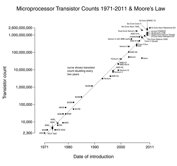
Fig. 1: Gordon Moore's prediction of transistor doubling on a yearly basis, made after seven years' worth of data and supposedly valid over only the next 10 years, has proven remarkably accurate over the subsequent nearly-50-year timespan.
In recent times, however, further extending the historical Moore's Law accomplishments has become increasingly challenging. Ever-thinner gate oxides translate into transistors that may never be fully “off,” with consequent ever-present leakage current that translates into clock speed-limiting high power consumption and consequent high heat dissipation (see Fig. 2 ).
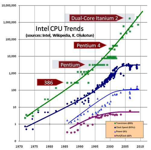
Fig. 2: Although transistor integration trends have held steady, power consumption has hit a thermal ceiling, thereby resulting in a tapering off of clock speed improvements over time.
Fortunately, continued advances in cost-effective single-die transistor integration have enabled microprocessors (for example) to advance beyond single-core historical approaches into multicore successors, in some cases composed of multiple interconnected CPUs and in others represented by SoCs that bundle a CPU, GPU, and other specialized processors. Unfortunately, though, algorithm and development toolset limitations have resulted in an incomplete harness of the multicore architectural potential.
Process tweaks
In responding to the power consumption crisis, “captive” fabs (owned and operated by IC suppliers such as Intel) and foundries alike have developed multiple versions of each process node, one (called LP, perhaps, for “low power”) with a thicker gate oxide and otherwise beefier transistor dimensions that limit leakage current at the tradeoff of comparatively slow switching speed, and the other (HP for “high performance,” for example) that boosts switching speed at the tradeoff of high power draw and heat generation.
It's even possible in some cases to fabricate both kinds of transistors on the same die. Nvidia partnered with TSMC, for example, to create the 40-nm process-based Tegra 3 SoC, which constructs the four primary ARM Cortex-A9 cores out of HP-fabricated circuits ( www.nvidia.com/content/PDF/tegra_white_papers/tegra-whitepaper-0911b.pdf) and the comparatively performance-uncritical remainder of the chip out of LP structures (see Fig. 3 ).
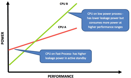
Fig. 3: Nvidia's ARM Cortex A9-based Tegra 3 SoC blends high-performance and low-power transistors on the same die.
Interconnect advancements
Historical IC design employed aluminum traces as the means of interconnecting transistors, with the insulating structures between transistors and/or interconnect traces fabricated out of conventional silicon dioxide. At the 130-nm node, Intel (a company which, as a leading process technology innovator, I'll repeatedly employ as a case study in this article although other fabs and foundries have often closely followed in its footsteps, sometimes even blazing a new breakthrough trail) made two notable interconnect advancements.
First, the company migrated its chips' interconnect from aluminum to copper, resulting in a more efficient conductor (both inherently and by virtue of copper's reduced electro-migration tendencies over time) but was complicated by the potential for copper atoms to corrupt the surrounding silicon lattice. A protective (but still conductive) barrier film between the copper interconnect structure and its silicon foundation is therefore required. And speaking of interconnections, as transistors (and interconnect traces, for that matter) nudge increasingly close together with reductions in process dimensions, in-between insulators' parasitic capacitance-induced signal propagation delays become increasingly apparent. A migration from conventional silicon dioxide insulators to a low-K dielectric counterpart (http://en.wikipedia.org/wiki/Low-k_dielectric) counteracts this phenomenon.
Silicon on insulator
Speaking of parasitic capacitance reductions, they're one of the key benefits touted by SoI (silicon on insulator) technology (http://en.wikipedia.org/wiki/Silicon_on_insulator), an approach which (at least to date) Intel has not chosen to implement in its high-volume manufacturing lines, but which other companies (such as AMD, beginning at 130 nm) have consistently-or-not embraced. SoI replaces an intermediary layer's worth of the bulk CMOS substrate on which an IC's transistors and other structures are sequentially built with a higher-insulation alternative such as silicon dioxide or (for radiation-intolerant applications) sapphire.
The earlier-mentioned reduction in parasitic capacitance, resulting from insulation-induced electrical isolation between the lowest bulk silicon level and the device circuitry, boosts performance or (said another way) reduces power consumption at equivalent performance to the 100%-bulk-silicon conventional approach. SoI backers also tout the approach's reduced preponderance of latch-up, resulting from more complete isolation of both n- and p-well circuit structures. However, you don't get something for nothing; SoI adds approximately 10% to 15% to the processing cost of each wafer's worth of ICs. And if ion implantation techniques are used to construct the silicon dioxide layer, they can also stress upper silicon regions, adversely affecting both initial manufacturing yield and long-term reliability.
Strained silicon
Beginning at the 90-nm process node, Intel instituted so-called “strained silicon” (http://en.wikipedia.org/wiki/Strained_silicon) into its high-volume manufacturing flow (see Fig. 4 ). Commonly implemented by means of a silicon germanium foundation layer, the aligned upper silicon layer's atoms' links are subsequently stretched beyond their normal inter-atomic distance by the larger native silicon germanium atom-to-atom span. This phenomenon reduces the atomic forces that limit electron flow through the silicon lattice, translating to up to 70% higher electron mobility and 35% higher transistor switching speeds.
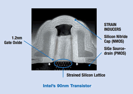
Fig. 4: Strained silicon uses a layer of silicon germanium or some other semiconductor blend to stretch the spacing between silicon atoms above, thereby resulting in increased electron mobility through the silicon lattice.
Hi-K dielectrics
While decreasing the dielectric constant of the insulator between transistors, interconnect traces, and other silicon-fabricated structures is generally a good thing, due to consequent reductions in parasitic capacitance, it's the exact opposite of the desired effect for the gate structure within a transistor. Especially as the gate dimensions shrink, retaining (if not boosting) a high dielectric constant is essential to ensuring that the transistor is as fully “off” as possible when desired, thereby limiting unnecessary and undesirable leakage current through the transistor caused by electron tunneling through the ever-thinner gate oxide.
Any of you who remember Intel's “Hafnium” promotional campaign (w ww.intel.com/content/www/us/en/silicon-innovations/intel-45nm-process-technology.html) associated with the company's 45-nm-based microprocessors have already been educated on the migration beyond conventional silicon dioxide gate materials to high-K dielectric counterparts (http://en.wikipedia.org/wiki/High-k_dielectric) conducted by Intel and its competitors, even if you don't yet realize it. Although such an approach may slightly boost cost, at least in the ramp-up phase of a process's lifespan, it's preferable to retaining a thick silicon-dioxide-based gate oxide, which would hamper transistor-switching performance.
Multigate transistors
Finally, we turn to another and more recent Intel promotional campaign, this one associated with the company's upcoming 22-nm process, the fabrication foundation for the initial Ivy Bridge CPUs ( http://en.wikipedia.org/wiki/Ivy_Bridge_(computer_processor)) scheduled to enter volume production later this year. Intel refers to the technique via the 3-D tri-gate transistor (http://newsroom.intel.com/docs/DOC-2032) marketing moniker (see Fig. 5 ). More generally, it's known in the industry as a multigate device (http://en.wikipedia.org/wiki/Multigate_device) or (specifically) a FinFET.
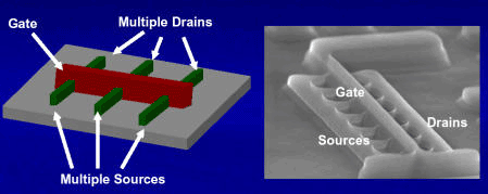
Fig. 5: A three-dimensional “fin” gate structure, which may be unique to each source-drain combination or shared among multiple source-drain sets, increases the effective gate surface area thereby leading to lower transistor power consumption and/or higher switching speeds.
Quoting from the Intel press release ( http://newsroom.intel.com/community/intel_newsroom/blog/2011/05/04/intel-reinvents-transistors-using-new-3-d-structure), “The 3-D Tri-Gate transistors are a reinvention of the transistor. The traditional ‘flat’ two-dimensional planar gate is replaced with an incredibly thin three-dimensional silicon fin that rises up vertically from the silicon substrate. Control of current is accomplished by implementing a gate on each of the three sides of the fin — two on each side and one across the top — rather than just one on top, as is the case with the 2-D planar transistor.
“The additional control enables as much transistor current flowing as possible when the transistor is in the ‘on’ state (for performance), and as close to zero as possible when it is in the ‘off’ state (to minimize power), and enables the transistor to switch very quickly between the two states (again, for performance).” To wit, Intel estimates, “the 22nm 3-D Tri-Gate transistors provide up to 37 percent performance increase at low voltage versus Intel's 32nm planar transistors…Alternatively, the new transistors consume less than half the power when at the same performance as 2-D planar transistors on 32nm chips.” ■
Advertisement
Learn more about Electronic Products Magazine


