Application Focus: RF and Microwave —Multilayer organics for high-frequency applications
Enabling RF components with higher Q values and high frequencies
BY GEORGE WHITE and
LARRY CARASTRO
AVX, www.avx.com
As the number of frequency bands continues to increase in electronic devices, such as smart phones, APs, net books and tablets, so does the requirement for higher Q and lower loss RF passive components. One such example can be illustrated in a multiband phone, which supports multiple wireless standards, such as Bluetooth, GSM, WLAN, GPS, and UMTS.
Most smart phones use multiple antennas to support each wireless frequency. Antennas add cost and provide interoperability challenges that can impact performance. To minimize the number of antennas for a multiband application, many designers incorporate low-loss high-Q RF components into their designs. These devices include capacitors for matching circuitry, inductors, and diplexers.
Tight tolerance high-Q low-loss capacitors, inductors, and diplexers can be used to improve isolation between bands, which can minimize the number of antennas, while enhancing performance and providing savings in both cost and size. A recently patented process called Multilayer Organics (MLOs) enables the development of RF components with considerably higher Q values at high frequencies than previously available.

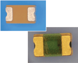
Fig 1: (a) MLO inductor. (b) MLO capacitor.
A typical MLO device substrate consists of one or more low-loss RF thin dielectric layers embedded between layers of other low-loss laminates to provide the effective shielding and routing necessary for a SMT device or IC substrate. Variations in the buildup of the MLO device can be used if thinner or thicker components are required. The dielectric layer must have low loss at the common wireless frequency ranges while at the same time exhibiting a high dielectric constant (Er) to provide high capacitance density.
Unfortunately, these are sometime counteracting properties for most material combinations, especially for ceramic based components when they are fabricated in a multilayer fashion. Organic devices have the advantage of being able to use disparate layers in a multilayer stack, while maintaining similar thermal expansion coefficients within the device. As a result, MLO-based SMD devices will have improved reliability from an assembly standpoint, since they exhibit little to no CTE differences.
Another key feature, and arguably one of the most important, is the ability to incorporate novel design topologies that take advantage of thin low-loss RF laminates. To derive the full benefits of the embedded device capabilities of MLOs, designers need the ability to rapidly implement the common components used in RF systems, such as tight tolerance capacitors, inductors, matching networks, filters, baluns, couplers, and diplexers. These components can be implemented in a wide range of circuit topologies, but must be ultimately transformed into lumped element structures consisting of embedded inductors, capacitors and transmission lines.
Manufacturers such as AVX have recently leveraged this capability with the announcement of a new line of tight tolerance, high-Q SMD inductors and capacitors (see Fig. 1 ). These best-in-class components, which leverage thin-film photolithographic techniques, can achieve extremely tight tolerances in small case sizes. MLO inductor components range in tolerance from ±0.1 nH to 5%, while MLO capacitors can achieve tolerances as tight as ± 0.05 pF.
MLO technology also allows for the realization of high-current- and high-voltage-handling capabilities when compared to conventional ceramic-based components. Inductor with Q values higher than 150 have been achieved at 3 GHz with MLO technology. This compares with Q values of 20 to 50 for silicon integrated passive devices or inductors fabricated on conventional FR4 laminates.
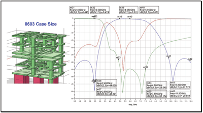
AVX continues to expand its offering of products using Multilayer Organic technology including a a new class of multiband diplexers using proprietary stackups and an extensive library of RF components. The device shown in Figure 2 is a 0603 unshielded dual-band WLAN diplexer slated for release for later this year.

Fig. 2: Unshielded WLAN diplexer.
The dual-band WLAN diplexer (2450.00 ± 50.00 MHz, 5250.00 ± 100.00 MHz) was initially synthesized using standard RF design tools and optimized to exceed specifications using an in-house custom design methodology.
This methodology uses an EM simulator such as Sonnet or Momentum to generate S-parameters, followed by use of ADS to create an electrical equivalent of the EM simulation. This allows the designer to globally optimize the electrical equivalent of the entire filter design, using a circuit analysis tool. The electrical equivalent then translates directly into layout creating a specification-compliant design.
As stated previously, this basic design can span case sizes and frequency bands. This is done by simply linearly scaling the internal components (to change frequencies), and/or re-using existing element values (for a smaller/larger case size). This flexibility allows design engineers to rapidly implement spec-compliant standard and custom designs. ■
Advertisement
Learn more about AVX


