Cost-effective devices fit high-speed data needs
BY NILADRI ROY, Sr.
Manager, Vertical Markets
and TED MARENA
Director, Business Development
Lattice Semiconductor
www.latticesemi.com
The image sensor is arguably the most important component in a digital video or still camera. But these sensors are also notoriously non-standardized. They tend to differ in the schemes used for:
1. The method employed to encode and sometimes compress the signal before getting it off the chip
2. The way in which registers inside the sensors must be programmed to adjust parameters
3. The way they implement specialized functions like high (or wide) dynamic range
4. The interfaces used to get the image signals to downstream processing logic
FPGAs provide a very cost-effective small footprint platform to easily convert signals from different image sensor interfaces to digital signals suitable for processing by downstream logic. They also provide a cost-effective programmable mechanism to adapt to a wide variety of devices.
Image sensor technologies
Image sensors fall into two broad classes: charge coupled device (CCD) sensors and complementary metal oxide semiconductor (CMOS) sensors. The majority of image sensors shipped today, by far, are CMOS sensors, and this article focuses exclusively on their interfaces.
There are several image sensor manufacturers of note today Aptina, OmniVision Technologies, Sony, Samsung, Panasonic, Toshiba, and Altasens, to name a few. As stated earlier, sensor manufacturers deploy a range of interfaces. It is entirely common for the same sensor manufacturer to use different interfaces, based on the amount of data that needs to be moved.
Modern sensors with megapixel resolution, for example, need to transfer out far more data than before and requirements like high dynamic range (HDR) also increase the amount of data that needs to be read from the image sensor per frame. The number of frames that need to be read in a given time, in order to support smoother low-latency high-quality video, also influence the choice of sensor interface.
Image sensor interface evolution
Until now, all sensors used a parallel LVCMOS interface, as shown in Fig. 1 . Sensors resolutions and frame rates have now increased to a point where the previously dominant CMOS parallel interface is no longer able to handle bandwidth requirements. Higher-speed sensors are using different interfaces to overcome the limitations of parallel LVCMOS. For example, Sony and Panasonic use parallel sub-LVDS interfaces, and OmniVision uses either MIPI or serial LVDS.
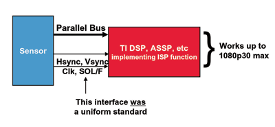
Fig. 1: Parallel LVCMOS image sensor interface.
Aptina Imaging has introduced a high-speed serial interface called HiSPi (High-Speed Serial Pixel Interface). The HiSPi interface can operate from one to four lanes of serial data, plus one clock lane. Each signal is sub-LVDS differential, centered at a common-mode voltage of 0.9 V. Each lane can run up to 700 Mbits/s.
Fig. 1: Parallel LVCMOS image sImage Sensor interface.I/F
HiSPi to parallel sensor interface bridging
Downstream video-processing logic devices have difficulty supporting many different sensor interfaces in an ASSP. The majority of image-signal-processing devices support traditional CMOS parallel sensor interfaces and lack support for high-speed ones.
Many of the parallel interfaces can run much faster than a sensor’s parallel interface, but since sensors have moved to various serial interfaces, the image processors need logic to translate to a parallel interface. An FPGA bridge device can convert the high-speed serial data to a parallel format. FPGAs provide simple, cost-effective programmable bridging between high-speed sensors and traditional image signal processing ASSPs (see Fig. 2 ).

Fig.2: Programmable bridge between high-speed image sensors and ASSP.
As a real-world example, the LatticeXP2-5 or MachX02 nonvolatile FPGA provides an efficient and cost-effective solution for bridging Aptina Imaging’s HiSPi serial interface to a Texas Instruments parallel interface DSP. This design interfaces an Aptina sensor with a HiSPi serial interface to a Texas Instruments TMS320DM3X5 that has a parallel interface. Evaluation hardware has been tested with Aptina’s sensors A-1000 sensorsMT9M034, AR0331, and MT9J003. The reference design supports packetized and streaming SP HiSPi formats from one to four lanes running up to 700 Mbits/s each. It also emulates parallel sensor output with 8-, 10-, 12-, 14-, or 16-bit bus widths. The parallel interface can be configured for 1.8-, 2.5-, or 3.3- V LVCMOS levels. A block diagram of the reference design is shown in Fig. 3 .
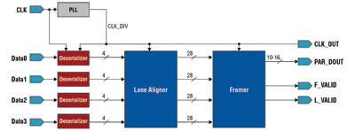
Fig. 3: Aptina HiSPi to TI DM385 interface bridge block diagram.
FPGA challenges in sensor interface bridging
The challenge for the FPGA here is that it must have sufficient I/O gearing logic to support the fast serial sensor interfaces and must provide a cost-effective small footprint. The LatticeXP2 or MachX02 used in our example has PLLs, dedicated edge clocks, and I/O-gearing logic to tackle the high-speed serial sensor interface. It can be as small as 8 x 8 mm and, due to its nonvolatile nature, the chip requires no boot PROM. The availability of image-signal-processing IP also enables larger LatticeXP2 devices to offer capabilities like sensor data linearization, sensor register programming, de-Bayering, defective pixel correction, gamma correction, and simple HDR up to 24 bits per color channel. ■
Advertisement
Learn more about Lattice Semiconductor


