Adding ESD protection for the latest high-speed USB systems need not be complex and confusing
BY PATRICK HIBBS, Sr. Global Strategic Market Manager,
TE Circuit Protection, a Business Unit of TE Connectivity
www.circuitprotection.com
When it was introduced in 1999, the USB 2.0 interface’s 480-Mbit/s half-duplex differential channel presented a challenge to designers implementing electrostatic discharge (ESD) protection when the range of low-capacitance, or “low-cap,” transient voltage suppressors (TVSs) comprised 1 to 1.2-pF discrete diodes. The subsequent USB 3.0, or SuperSpeed USB, interface maintains the exact physical 2.0 interface, and complicates the protection problem by adding two 5-Gbit/s half-duplex differential pairs (one Tx and one Rx pair).
The rapid increase in the bandwidth to the connectors created another protection challenge; the chipset’s interface speeds increased and silicon feature sizes decreased. This combination of faster speed and smaller I/O cells led to increased ESD susceptibility for the chipset’s PHY I/O’s, while limiting the external impedance-loading budget to the point where low-cap ESD was no longer low enough. As a result, designers have transitioned from copying and pasting generic discrete ESD component layouts into new designs to performing careful board characterization with respect to timing, matched impedances, and insertion loss.
ESD protection for USB 3.0
When adding ESD protection to USB 3.0 systems, it is essential to consider the potential impact of additional capacitance and inductance on the timing of the chosen device on the high-speed differential pairs. When operating at 5 Gbits/s on each of the SuperSpeed USB differential pairs, any additional impedance on the line can distort the signal, leading to greater difficulty in meeting the required eye diagrams for rise times and signal levels, additional constraints on board design, lower system-level performance, and interoperability issues with different cables (quality and length).
To minimize timing impact on these high-speed lines, and to provide adequate protection to the downstream chipset, there are technical considerations to be made regarding the ESD protection device, as discussed in the following sections.
Low capacitance, low insertion loss
Any physical protection device placed on a circuit node will add parasitic electrical elements to the system. Even the routing of an ideal clamp device can create unavoidable disturbances in the PCB trace geometry, including parasitic capacitance created by the plate capacitor formed on the PCB by the solder pad, inductive discontinuities caused by fan-in/fan-out routing bends, or unavoidable vias.
When reviewing specifications for TVSs, some common characteristic parameters are listed primarily as a historical legacy of lab measurements, rather than as data which has been collected specifically to make the system designer’s choice easier and more comprehensive. For example, input capacitance (CIN) or channel capacitance (CCH) are often specified at 1 MHz because earlier discrete and logic devices were measured with 1-MHz LCR meters. While it is not likely to find a 1-MHz capacitance measurement for a 5-GBit/s PHY I/O pin, it may be surprising to find such a measurement for a device targeted for that application.
So rather than trying to overlay a legacy capacitance value over a cutting-edge application, it is more productive to consider the impedance and insertion loss due to the device in the circuit at the frequencies and harmonics of interest (beyond hundreds of megahertz and gigahertz for USB 3.0).
For selection of a single passive component within a channel, insertion loss characterization reveals the primary relevant contributions of parasitic effects on the channel for that device. It can be noted in Fig. 1 that the insertion loss measurement of the silicon ESD (SESD) device is limited to 6 GHz due to measurement equipment limitations, just short of the 7.5- and 12.5-GHz third and fifth harmonics in USB 3.0. Indeed at some point any TVS device will exhibit a self-resonance where the primary channel capacitance and the bondwire inductance will nullify the insertion loss. After this point, the bondwire inductance will tend to isolate the parasitic capacitance from loading the channel.
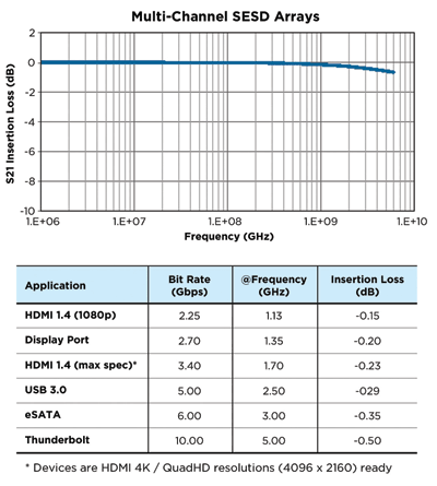
Fig. 1: An example of single-ended insertion loss of a silicon ESD (SESD) device.
ESD robustness
In general, an overall system is only as robust as its weakest elements. On each node the current sharing of each device will naturally select the least robust component for first failure during an ESD strike. In the most simplified example of modeling destructive behavior (see Fig. 2 ), a TVS device and the I/O structure of the protected ASIC are modeled as simple diode clamps connected with the lumped element or transmission line of a PCB trace.
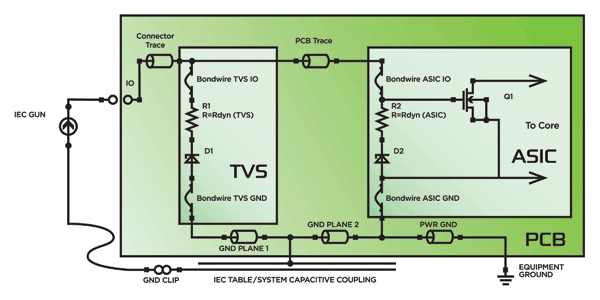
Fig. 2: Simplified ESD PCB high-current discharge paths (IEC bleed resistors omitted for clarity).
The protection objective of external TVS clamps, such as SESD devices, is to divert sufficient current from the ESD pulse applied to the system through the TVS clamp (ITVS) such that the residual current (IASIC) and clamped voltage levels can be tolerated by the ASIC without damage (“hard failure”) and, if possible, without a system upset (“soft failure”).
Protection circuits fabricated in deep submicron ASIC technology are inherently fast and clamp at very low voltages; but the fine geometry also limits the physical clamp dimensions and thus the total clamp power handling capability. (Note: Care must be given during board layout to place the TVS as close to the connector (or the ingress point of potential ESD damage), and as far away from the protected ASIC as possible.) This layout is common in board design to have sufficient impedance between the TVS and the ASIC so transient energy is diverted to the TVS clamp.
ESD robustness in the real world relies on an assumption about the margin of safety and the probabilistic distribution of strike event energy over time. If a device survives a bare minimum 10 test strikes at 8 kV, this information does not offer a clear indication about its robustness. For instance, the device may not survive an 11th strike at 8 kV, and it may not even survive an 11th strike at 3 kV.
An attempt has been made by the industry to extend the confidence of the characterization with multi-strike capability, or qualifications of 1,000 consecutive strikes at a given robustness level to demonstrate a lifetime of repeatability. If an ESD device or an ASIC’s I/O cell shorts due to localized filaments or subsequent EOS before the metallization fails, then the device may fail short.
If the device fails after a short damages an interconnect in the device, then the result may be open. If the device fails short, then the ASIC is protected from further strikes, but the system port functionality may be disabled. If the device fails open, the next strike will most certainly damage the ASIC I/O and may permanently damage larger parts of the ASIC. In the case of a core logic chip with integrated USB 3.0 ports, this may mean an entire system is rendered inoperable.
Smaller device packages
Packaging development has also been a key design factor in ESD protection. SOT-23 and MSOP-10 plastic packages, once the mainstay of TVS components, are now considered unacceptable for low-cap applications such as USB 3.0. The traditional packages, previously thought to be compact, require PCB pad sizes that inherently contribute as much or more parasitic capacitance even before the TVS device is populated.
To meet the requirements of today’s leading high-speed applications, silicon ESD devices must take into account the applications’ pad sizes and PCB routing difficulties. This has driven the need for flow-through layouts. Also, to meet the applications’ timing and insertion loss requirements, today’s highest-performance silicon ESD devices have reduced their package sizes to save board space and mitigate the parasitic effects of long inductive lead frames and bondwires (see Fig. 3 ).
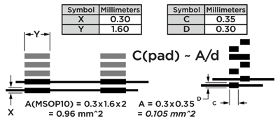
Fig. 3: New SESD packages provide 2/3 reduction in pad area and capacitance.
When designing SuperSpeed USB systems, adding ESD protection need not be a complex and confusing task. New silicon ESD devices offer low-capacitance, high-ESD kilovolt rating for low-cap devices as well as small flow-through arrays. For USB 3.0, an effective solution can be to use a single six-channel array when protecting only the six high-bandwidth lines. If the system requirement is to protect all eight lines. ■
Advertisement
Learn more about TE Circuit Protection Group


