Characterizing power devices from lab to fab
Testing higher-performance power devices with gear that’s no longer up to the job is placing a growing burden on designers
BY LEE STAUFFER
Senior Staff Technologist
Keithley Instruments
www.keithley.com
The recent drive toward greater energy efficiency has created an increasing demand for better high-power semiconductor devices such as diodes, FETs, IGBTs, and others. New technologies hold the promise of higher performance, including lower on-state losses, lower off-state leakage, faster switching, and reduced loss while switching.
However, along with the improved performance of these devices, characterization and measurements are becoming more complex and difficult In this article, we will examine a typical workflow in the design and development of a power semiconductor device and discuss some of the equipment and measurement challenges associated with them.
Concurrent processes
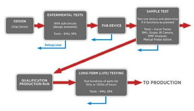
With some of the newer technologies, the fabrication process is often being developed at the same time as the devices themselves (see Fig. 1 ).

Fig. 1: Typical power semiconductor design and development lab-to-fab workflow.
In some cases, the device designer will have the fab create simple sub-circuits to test some element of the process. These devices include simple Schottky and bipolar diodes, and even resistors and capacitors.
Testing at this level usually involves I-V (current-voltage) characterization with a simple curve tracer. The designer wants an instrument that is very quick and easy to set up, with interactive control of the voltage and current levels, and fast feedback on the display to allow quick determination of proper voltage limits. Given that exceptional measurement accuracy and sensitivity are typically not critical to such applications, curve tracers remain well suited to this task.
The next step (or the first step in many situations) is to fabricate a real device. Characterization on this device starts out with taking a simple I-V (current-voltage) curve to determine basic device characteristics. Usually, the designer knows what he or she expects the device to do but not what the device actually does. Again, a curve tracer can be a simple and efficient choice for this task. It allows the designer to apply a controlled voltage carefully, read back the current to determine if junctions and interconnects designed actually exist, and discover the typical breakdown voltage or on-current the device can handle.
Connecting a curve tracer safely to a probe station is a common test problem in this situation. Curve tracers were typically intended to test packaged parts, it is much more efficient to test devices on the wafer directly, eliminating the cost and time of packaging the part. The newest generation of source measurement units, or SMUs (including Keithley’s Models 2651A and 2657A High Power System SourceMeter instruments), provide safer and more accurate connections, and better control over the voltage and current.
The designer can control the instrument using the front panel knob and display or via the LXI-compliant web page embedded in the instrument. Another option is to connect the instrument to an external controller running an application created using something like Keithley’s ACS Basic Edition Test Software for Component and Discrete Devices, which provides a simple trace mode that provides precise control of the voltage and readback of the current.
Parameter checks
Drain breakdown voltage (BVDSS ) is one parameter commonly checked during fabrication of experimental devices. When checking BVDSS manually, the voltage is slowly increased until a target current is reached.
A faster, more-efficient way to make this measurement is to source the target current and read the voltage at which the device settles. This requires an instrument that provides both an accurate, fast-acting voltage meter and a voltage clamp. Because this test is often performed using pulsed test signals, the user must make certain that the voltage has settled to a final value before taking the reading. The newest SMUs combine fast settling with fast digitizers to allow the designer to verify these breakdown measurements are valid.
Another important parameter is the drain and gate leakage currents. On older silicon technologies, the leakage could be many microamperes, but the newer silicon carbide and gallium nitride materials exhibit much lower leakage.
Measuring nanoamperes or even picoamperes accurately requires both an instrument that has sufficient sensitivity and the proper cables and connections. In this context, “proper” cables means triaxial cables and a driven guard, features that were never available with earlier generations of high-voltage test equipment. Triaxial cables not only minimize stray leakage currents, but they shield the measurement from noise and allow the test signal to settle much more quickly.
On-state resistance (RDS(on) ) is an important measurement but often a difficult one to make accurately. Typical sources of error in this measurement include the sensitivity (or lack thereof) of the voltage measurement, the noise level, and the difficulty of compensating for drops in the test leads.
Given that RDS(on) could be as low as a few milliohms, very little voltage is generated even when the currents are as high as 50 A or more. Curve tracers simply can’t provide sufficient voltage sensitivity. In some cases, users have attempted to create test solutions by integrating power supplies and sensitive voltmeters, but these solutions are typically limited by synchronization and settling time problems. Most devices can only handle high currents for very short periods, perhaps just hundreds of milliseconds. All it takes is a little extra stray inductance in the test cables to extend the measurement’s settling time, creating inaccurate results.
The threshold voltage of the transistor has some interesting test challenges associated with it as well. For example, one way of measuring threshold voltage is to hold the drain at a fixed bias while sweeping the gate and measuring the resultant drain current. However, the drain actually needs to be in a pulse mode to prevent the device from heating up, which would cause a shift in the device’s characteristics.
In any pulse test, in order to make accurate, repeatable measurements, it is imperative for users to make certain that the entire test system has reached a settled state. Recently, we encountered an interesting problem with an inaccuracy in the gate voltage measurement caused by the residual resistance in the test leads connected to the source of the device. The large pulse of current flowing from the drain to the source caused the source terminal voltage to increase with respect to the gate, thereby reducing the gate drive and causing an error. After repositioning the gate sense leads to be directly on the source, we were able to eliminate the error.
Fab feedback
In some cases, designers use the initial data they obtain to provide feedback to the fab, requesting a tweak of some process parameter, the better to establish the particular device characteristic for which they are looking.
Once the designer is satisfied the device is ready, he or she moves on to a much more detailed sample testing phase. In addition to static dc I-V tests, this stage of characterization includes ac impedance parameters, such as various device capacitances (such as CISS , COSS , CRSS ). Capacitance can be a tricky measurement in as much as all of the stray impedances in the cables and test fixtures need to be properly compensated. This is usually done with an open and short correction step, but it can be difficult to simulate the open and short conditions in a power device test fixture or probe station. Coaxial cables should be used, and extra care should be taken to make sure the shields of the cables are connected together as close to the device as possible.
Designers also typically measure several other ac and transient characteristics, including rise/fall time (tr, tf ), switching delay (tdon , tdoff ) and reverse recovery time (trr ). For power FETs and IGBTs, numerous charge measurements are performed, including total gate charge (QG ), pre- and post-threshold gate charge (QGS1 , QGS2 ), drain charge (QGD ) and output charge (QOSS ). This is usually done with a combination of sources, oscilloscopes and probes.
Curve tracers’ limited applicability becomes increasingly apparent and they have been largely replaced with modern digital semiconductor parameter analyzers (SPAs) for these types of measurements. Until recently, even SPAs were limited by insufficient power and capability for such applications. For example, many lacked the speed or power necessary to capture many of the charge characteristics.
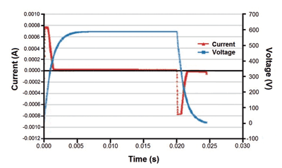
A difficult test called “dynamic on resistance” (sometimes referred to as “current collapse” in a gallium nitride power HEMT) is one good example. The device must be biased to full breakdown voltage, typically 600 V, then switched to full on-current, often as high as 50 A, all while monitoring the on-resistance for rapid changes in RDS(on) . These changes can occur as rapidly as microseconds and can continue for milliseconds. The latest high-power SMUs incorporate numerous digital enhancements, such as high-speed digitizers, intended to make it easier for designers to capture important data (see Fig. 2 ). Other equipment used at the sample testing stage includes pulse generators and oscilloscopes, IR cameras, EMF test, and wafer probers. In some cases, the devices will be packaged to allow for easier testing in a specially designed test fixture rather than at the wafer level.

Fig. 2: This high-voltage pulse shows unsettled current transients.
Ramping up
Once sample testing is complete, the designer moves on to statistical sample testing. The number of devices tested and the volume generated usually requires the use of a much more automated process.
Although there are several vendors of automated power device test systems, such systems are expensive and the scope of the tests they can perform is often limited. For example, typical drain leakage currents on a silicon carbide power FET might be less than 1 nA, but an automated power device tester is often limited to hundreds of nanoamperes or even microampere capability.
One solution is for the power device manufacturer to configure their own automated solutions using higher performance instrumentation, such as the latest high power SMUs, which now offer numerous features designed to simplify the development of automated systems, including built-in scripting capability, and virtual backplane capability for synchronizing multiple instruments for more complex solutions. Keithley offers software specifically designed to control and manage automated testers; Automated Characterization Suite (ACS) software was specifically designed to manage data acquisition and data management across multiple devices undergoing multiple tests.
Once a designer is satisfied that a statistical sample of the devices perform as required, the next step is a production qualification run. From these wafers, a long-term (life) test can be set up to validate the reliability of the devices under different conditions designed to emulate the real world. This is normally done in large parallel batches, with many devices installed in thermally controlled environments. Many hundreds of devices are tested for hundreds or thousands of hours under various electrical and environmental stress conditions.
In most cases, the designer has specific conditions that he wants life-tested, which makes it essential that the test equipment be flexible and readily reconfigurable. Creating and maintaining parallel test resources and monitoring and managing the masses of data acquired during this phase can easily become overwhelming. Typical parameters tested here include leakage current (IDSS and IGSS ), on resistance (RDS(on) ), and threshold voltage drift (delta VTH ).
Correlating the results of tests performed in various test environments has always been complicated due in no small part to the very different test systems (each with its own unique set of capabilities and sources of error) often used in different test environments. Today, a growing number of device manufacturers are striving to converge on a uniform instrumentation set so that, for example, the leakage current measurements made in the early stages of device design can be correlated with those from devices being produced the fab. ■
Advertisement
Learn more about Keithley Instruments


