Quality and verification considerations for digital power modules
The impact of highly configurable digital power supplies falls upon quality assurance something that was foreign to analog-converter environments
BY PATRICK LE FÈVRE
Marketing and Communications Director
Ericsson Power Modules
www.ericsson.com
Digitally controlled and managed power supplies represent a rapidly growing part of the power conversion industry: They are breaking out of the telecom/datacom markets and into other mainstream applications where the superior performance and reliability of distributed power can deliver major benefits. And there are many advantages offered by digital inner-loop control and integrated power-management subsystems over conventional analog control.
However, the full impact of highly configurable digital power supplies extends beyond immediately obvious boundaries. A key impact falls upon quality assurance (QA) processes, which must accommodate parameters and processes that were formerly alien to analog-converter environments.
Digital control
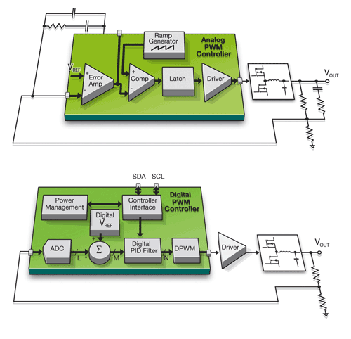
Figure 1 compares the differences between analog and digital control methodologies. Much of the converter’s hardware remains essentially unchanged, such as the filtering, magnetics and power semiconductors. What changes is the method of PWM control, such as where a buck converter varies the duty cycle of the top (control) MOSFET and the lower (sync) switch.

Fig 1: A digital buck converter substitutes digital-signal-processing techniques for the traditional analog control loop.
The digital power converter abandons analog control-loop dynamics for a system that converts the feedback error-signal into numbers that are compared in a digital summing amplifier, filtered in a proportional-integral-differential (PID) filter, and then fed into a logic block optimized for high-speed, high-resolution PWM generation.
The regular QA model for analog power supplies is also broken by the flexibility of onboard firmware, which allows the programming of multiple parameters to determine the converter’s operational behavior. The algorithms that control the digital core are generally “factory set” and reside in protected on-chip nonvolatile memory. Depending upon the converter’s implementation, key parameters may be available for modification — such as the dead-time between the MOSFETs switching, which has a profound effect upon conversion efficiency across the line/load spectrum, and the digital PID filter constants that balance stability and transient response for a given downconversion ratio and load bulk capacitance.
Hardware, firmware, and software
The operation of firmware is hard to assess without access to a well-developed test suite that exercises every part of the code’s range; and this challenge becomes increasingly difficult with an extra ‘software’ layer of custom parameters. The underlying physical logic is ‘hardware’ and depending upon the depth of the QA regime, concerns may range from assuring data retention in on-chip memory to ensuring that logic block elements and the microcontroller perform as expected under all foreseeable conditions. In addition, there is the application software that runs the end-user’s product.
Hardware/firmware robustness is invariably extremely high, yet a product may occasionally fail in unusual circumstances such as when the system designer fails to observe a critical boundary condition. Such conditions may include excessive dV/dT at the power converter’s input, which might occur during power-up due to uncontrolled inrush currents or during operation if transients strike the part.
Application-specific code that appears in an end product may be more challenging to assess. This code typically contains operating parameters that affect the power supply’s feedback control loop, including output voltage settings, and may include constants that directly affect the digital filter and other key hardware elements that could compromise the converter’s stability.
Each digital power supply can operate over a broad range of parameters. As part of the design and manufacturing process of an off-the-shelf digital power supply, default settings are defined, programmed into the product, and verified before shipment. In addition, several key settings are tested to ensure that the product operates reliably over its intended functional range. Clearly, there is a software element that is necessary to program and exercise the product during its manufacturing process, which is originally the responsibility of the power-supply maker. Yet the flexibility that digital supplies offer means that OEMs or even component distributors may re-program the supply. This means that their software and processes become an integral element of the QA inspection regime.
Material sourcing
Digital power introduces some new challenges in terms of the power-control chip: almost invariably a complex mixed-signal device and specific to a single semiconductor maker. Key to this is working closely with semiconductor partners to develop parts and ensure their availability — a second source is an option, but only sometimes. These are just some of the points to consider:
• Two or more equivalent manufacturing sites for the vendor’s ICs
• Highly robust nonvolatile memory and communication interface
• Built-in fault detection and diagnostic capability
• Extensive QA testing during IC design and manufacture
• Level control for firmware that’s loaded during IC manufacture
• Rigorous control of logistics flow during IC manufacture and shipment
Design verification testing
Design Verification Testing (DVT) is performed close to the end of a product’s design cycle to ensure that the product meets all of its design specifications in terms of functionality and performance. For an analog supply, there are well-defined parameters such as output voltage stability versus current drive and operating temperature range and so on, but for digital power, DVT also applies to the firmware content within the product, much of which is proprietary to the power module supplier. Essentially, the firmware makes it possible to define an almost infinite number of products that use an identical hardware base. This results in an exponential increase in DVT complexity. Ericsson solves this conundrum with an intelligent DVT concept that considers the expected application profile of each product and tests accordingly.
Another area is the electromagnetic susceptibility (EMS) performance of the controller chip and its memory. These are small-geometry ICs that are critical to the operation of the power supply and they live in close proximity to the large currents and electromagnetic fields that accompany any switching power supply of more than a few tens of watts. Their robustness in such an environment must be carefully verified so that data integrity is not compromised.
Qualification
Qualification tests ensure that the design and manufacturing processes result in a product that provides long-term reliability under all environmental conditions of interest. Such tests may be made at various levels within the end product’s process flow — initially at the component supplier and then at final board test with functional testing via ATE.
In terms of the long-term performance of the microcontroller and its memory with regard to software data integrity, the semiconductor industry has made enormous efforts in developing radiation-hard MIL-spec components and applying its knowledge to everyday components. Of course, there is a balance to strike between MIL-spec testing that examines every component under every conceivable operational condition versus making highly reliable products available at affordable cost. Obvious tests for memory-based digital products include write endurance and data retention and in theory at least, these parameters should be guaranteed by design and far exceed the product’s expected lifetime.
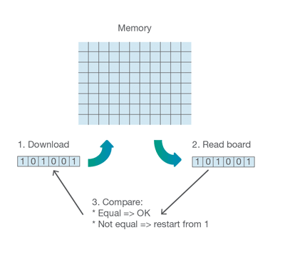
Among other reliability assurance checks, as an example, Ericsson tests the data retention and integrity of on-chip memories by comparing the memory content before and after conventional hardware environmental tests, such as 1,000 hours at 85°C/85% RH (see Fig 2 ).

Fig. 2: A readback-and-compare routine ensures memory integrity.
Manufacturing
The ultimate mission for QA is to eliminate all risks to ensure that customers receive their products on time, every time, and always within specification. This is what any holistic QA regime strives to achieve — “making it right first time, every time” saves time and expense.
The changes to conventional manufacturing processes to accommodate digital power products are minor, and primarily relate to programming parts during manufacture — an insignificant consideration given the predominance of today’s ATE systems — yet it can be easy for people to overlook the importance of simple points such as tracking version control for firmware/software elements.
Upgrades
And finally, any holistic QA regime embraces the period after the base product leaves the factory and ideally tracks it through its entire lifecycle. Often, enhancements to the firmware/software will occur following deployment. These changes could be driven by improvements that the power supply manufacturer develops, or the result of specific customer requests and ongoing development by the OEM. It is therefore important to have a reliable QA system in place for managing software changes and any upgrade activities. ■
Advertisement
Learn more about Ericsson Power Modules


