Maximizing buck regulator efficiency with a soft-switching topology
Regulation from a higher voltage, at a higher efficiency, and in a smaller form factor is realizable when the switching topology is improved
BY CHRIS R. SWARTZ
Principal Engineer
Vicor
Andover, MA
www.vicor.com
Buck regulators have evolved based on application and system power demands. Be it automotive, computing, industrial, military they all drive for higher power requirements. Regulators have evolved improving upon power throughput, efficiency, and size. The limiting factor with this improvement progression is reducing the regulator switching losses that only grow with higher input voltage or switching frequency. These switching losses prevent dramatic improvements in overall power system solutions. For example, within industrial process control systems a desired regulation of 24 to 3.3 V may be achieved by first regulating from 24 V to 12 V followed by a second regulator converting 12 V to 3.3 V. In contrast, by having a single regulation stage that can regulate 24 V to 3.3 V with an efficiency level at or higher than the two stages would dramatically improve cost, board space, and reliability.
Increasing the voltage input of a regulator to a higher-voltage input typically results in a dramatic reduction in efficiency, which is why most engineers use a two-stage approach for high Vin to point of load applications. This reduced efficiency is attributed to the regulator’s MOSFET switching losses. A higher-voltage input and/or current translates to higher losses within the MOSFET. These switching losses also increase with higher switching frequency, further hindering a regulator’s performance. Miller gate charge and body diode conduction losses also contribute to efficiency losses that also increase with higher Vin and/or higher switching frequency.
Advances in silicon integration, MOSFET technology and packaging have provided improvements for higher-Vin regulators. However, to achieve greater levels of performance, a soft-switching topology also needs to be used vs. a conventional hard switching topology. Implementing a soft-switching technology, like zero-voltage switching (ZVS), directly reduces switching losses by practically eliminating the voltage across the MOSFET during turn on. The result of lower switching losses is the desired regulation of higher input voltages at higher efficiency levels. Also, with the lower switching losses enabling higher-frequency operation, overall size of the regulator solution can be further reduced.
ZVS switching topology in buck regulators
ZVS topology is typically associated with high-performance isolated power supplies. Let’s consider silicon integration of a ZVS soft-switching topology within a buck regulator which provides several advantages. Let’s look first at efficiency.
Fig. 1 shows efficiency performance with a 24-V input revealing efficiency performance 5% to 10% over typical hard-switching high-density buck regulators that switch at much lower frequency. Translated to power loss, the soft-switching buck regulator has a 50% to 60% improvement in power-loss performance over lower switching frequency converters. The improvement is much greater when comparing conventional converters switching at very high frequency. Lower power loss results in less package temperature rise generated for the same amount of power throughput, creating a higher-power-density form factor. These means that the designer can replace a two stage regulation with a single stage ZVS regulation and achieve performance at or better than the two-stage conversion.
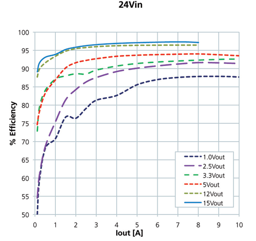
Fig. 1: Efficiency performance of Picor Cool-Power ZVS buck regulator for 24-V input
Referring to Fig. 2 , a direct comparison can be made between a typical Buck Topology and the new ZVS Buck Topology. Starting first with the typical approach at the start of a complete switching cycle (denoted by the yellow bar), the high-side MOSFET is commanded to turn on. Just prior to turn on, there is inductor current flowing in the output inductor and the synchronous MOSFET. In order to avoid cross conduction of the MOSFET’s, there is a delicate balance between turning off the synchronous MOSFET and turning on the high-side MOSFET.
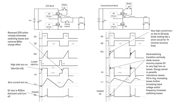
Fig. 2: Comparison of conventional and ZVS buck topologies.
The result of this design tradeoff is often body diode conduction. Conduction of the body diode requires that the stored charge accumulated while it is conducting at some peak current be swept away before the diode can support any reverse blocking voltage. As such, the drain to source voltage of the MOSFET is practically clamped at the input voltage (strongly dependent on parasitic inductance) while very high current flows through the body diode and through the high-side MOSFET until a depletion region forms and the body diode starts to support reverse voltage.
Until that time, the instantaneous power dissipated in the high-side MOSFET is quite high. Part of the losses are incurred due to the reverse recovery current and the rest are due to discharging the MOSFET output capacitance. In addition, there are reverse recovery losses in the low-side synchronous MOSFET body diode as well. These losses increase with increases in switching frequency or input voltage. The power curve for Q1 in Fig. 3 for the conventional buck regulator shows the effect of turn on. The peak instantaneous power at turn-on can be a dominant loss contributor for the high-side MOSFET in high-switching-frequency applications. There have been attempts to remedy the switching loss associated with body diode conduction ranging from switching faster to adaptive gate drivers and even MOSFET improvement through various improved Figure Of Merit (FOM) devices.
The ZVS Buck Topology starts it’s switching cycle with nearly zero current flowing in the output inductor. The voltage across Q1 is nearly zero as a result of ZVS action and the inductor current ramps up from zero to a peak value followed by Q1 turning off. The inductor current is commutated to the Q2 body diode for under 10ns and Q2 turns on. The stored energy in the inductor is delivered to the load. The turn off of Q2 is delayed until the inductor current is driven negative by current from the output capacitor, storing energy in the inductor.
Next, the clamp switch turns on, allowing the stored energy to circulate until Q1 needs to turn on again and clamping VS to Vout. To facilitate ZVS, the clamp switch opens. The stored energy then resonates with the output capacitance of Q1 and Q2. Resonant current flows into Q1 from S to D and into Q2 from D-S. This resonant action discharges Q1’s output capacitance and charges Q2’s output capacitance. Then Q1 can turn in a lossless manner.
The ZVS Buck topology addresses the high turn on losses of the conventional converter by eliminating high current body diode conduction prior to turn on of the high-side MOSFET, ringing the D-S voltage of the high-side MOSFET to zero or nearly zero and produces no high current spikes or damaging ringing. The ZVS action applied to Q1 removes the Miller effect at turn on of Q1, allowing the use of a smaller driver and lower gate drive at turn on.
The lower switching losses of the ZVS buck regulator also enable a higher switching frequency that is typically 2x to 3x that of conventional hard switching regulators. This higher-frequency operation contributes to a higher density form factor with smaller passive components utilized.
See Fig. 3 . Higher-frequency operation also reduces the burden on external filtering components and allows for fast dynamic response to line and load transients.
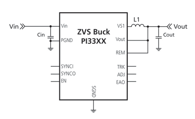
Fig. 3: The integrated high-voltage ZVS buck regulator requires only input/output capacitors and an output inductor to complete the design of a step-down switch-mode dc/dc converter.
Regulation from a higher voltage, at a higher efficiency, and in a smaller form factor is realizable when improving upon the switching topology used. The PI33xx demonstrates regulation up to 36 Vin with performance greater than that of conventional hard-switching high-density regulators. ■
Advertisement
Learn more about Vicor


