Simulating electrical noise from power supplies
Characterizing a design’s ability to reject/attenuate supply noise is critical, because such noise can appear as various errors
BY NEIL FORCIER
Application Engineer
Agilent Technologies
www.agilent.com
Designs ranging from transceiver chips for smartphones to radar assemblies for fighter jets require power-supply noise immunity testing, which is often referred to as power-supply rejection ratio (PSRR) testing. Characterizing the design’s ability to reject or attenuate supply noise is critical because the noise can manifest itself as bit errors in the case of transceiver chips and inaccurate target data in the case of radar assemblies.
Testing PSRR includes generating high-frequency noise signals on power-supply levels. This task is challenging due to the high capacitance present at most power-supply inputs. In this article, we look at two economical methods of testing PSRR.
Simulation challenges
When you test PSRR, one challenge is modulating a quantitative noise signal onto a dc power-supply level. This task is difficult because the power-supply inputs typically present extremely low input impedance to any ac signal as a result of the high input parallel capacitance.
While modern high-performance test and measurement power supplies do have built-in arbitrary waveform capability, the output bandwidth of power-supply waveforms is typically limited to less than 30 kHz. This limitation only allows you to simulate low-frequency noise sources, such as power line ripple. It falls well short of the more critical noise source frequency ranges, such as power-supply switching noise which ranges from 50 kHz to greater than 20 MHz.
To put the first challenge in perspective, let’s consider an example transceiver chip for a smartphone. The power-supply input most likely has a parallel 1-μF bypass ceramic capacitor as well as a large 10-μF electrolytic capacitor to serve as an energy reservoir for the sharp transmit transients. That means a 1-MHz sine wave modulated onto the power-supply level of the RF power amplifier would, in theory, only see a load of less than 20 mΩ. In practice, the equivalent series resistance (ESR), equivalent series inductance (ESL), and other parasitic impedances boost the load impedance up to more than 50 mΩ, but that still presents low input impedance to any ac signal content.
Let’s look at two solutions for simulating power-supply noise The Op amp/MOSFET Solution (TOMS) and The Amplified Modulation Solution (TAMS) — that use (for the most part) general-purpose test equipment and simple components that you can find around the office or lab.
TOMS
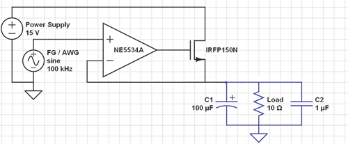
TOMS (see Fig. 1 ) requires two power supplies, a function/arbitrary waveform generator (FG/AWG), an op amp, and a high-power n-type MOSFET. TOMS uses the MOSFET as a variable resistor between the power supply and the DUT (load). By varying the MOSFET’s drain to source resistance we can modulate the power supply’s dc level with the desired noise signal.

Fig. 1: In TOMS circuit, C1, C2, and the resistance value labeled “Load” represent the device under test’s power supply input.
The op amp is used to maintain the desired voltage level at the DUT. With the op amp’s inverting input connected to the same node as the input to the load, the op amp will drive the MOSFET’s gate such that the amplitude level at its inverting input is the same as the amplitude at its non-inverting input.
The FG/AWG’s output creates the amplitude level and noise signal at the DUT’s input. The power supply’s output voltage should be set comfortably higher than the desired amplitude plus any added noise signal amplitude to ensure the MOSFET stays properly biased. TOMS circuit allows you to accurately generate noise signals with bandwidths up to about 500 kHz. The bandwidth can vary depending on the DUT’s input impedance and how well TOMS circuit was constructed. For best results, keep wiring and leads as short as possible to prevent oscillations.
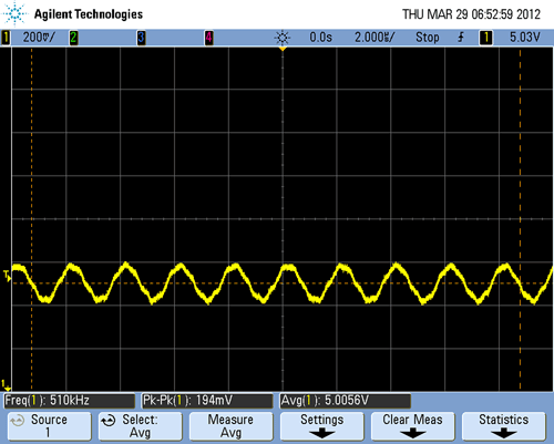
As an example, TOMS circuit was implemented using a 33521A function/arbitrary waveform generator, N6762A power supply, E3630A dual-output power supply (to power the op amp), an IRFP150N N-type MOSFET, and an NE5534A op amp to generate a 200-mVp-p 500-kHz sine wave onto a 5-Vdc level (see Fig. 2 ). The same DUT load shown in Fig. 1 was used for the example, with an electrolytic 100-μF C1 capacitor and a ceramic 1-μF C2 capacitor.

Fig. 2: The 500-kHz sine-wave signal on top of a dc level was generated by TOMS.
When you implement TOMS, you will need to use a high-performance power supply because you need a supply with a fast transient response and a stable output to ensure the supply can handle the rapidly varying load levels caused by the noise signal. Also, in TOMS, the dc level value is limited to the max voltage of the FG/AWG, which today is typically 10 V. To overcome this limitation, you could add a voltage amplifier between the op amp and the FG/AWG.
TAMS
TAMS (see Fig. 3 ) does not have the voltage or bandwidth limitations that TOMS has, but it does have a higher price tag. TAMS consists of a power supply, function generator/arbitrary waveform generator (FG/AWG) or signal generator, wide-band or RF power amplifier, and coupling capacitor section.

Fig. 3: TAMS circuit shown here is more expensive to implement, but it is also more capable.
The FG/AWG and RF amp are used to modulate the dc level from the power supply with the desired noise signal. The coupling capacitor section blocks the dc level from the RF amp’s input and provides a low-impedance path for the ac output of the power amp. The power amplifier is needed to boost the noise-signal power to deal with the low ac impedance that the DUT’s input presents.
You’ll want to make sure the coupling capacitor section’s impedance is as low as possible, so you may want to use multiple capacitor values and types in parallel to reduce the effects of ESR and ESL. The exact circuit setup, the DUT’s true input impedance, and the bandwidth of the noise signal will all determine how many watts the RF amp should be.
A good place to start is 10 W, and you can go up from there. Note that the RF amp’s output impedance should be as low as possible, which is typically going to be 50 Ω. With the DUT’s impedance being so low, the RF amp will see a large amount of reflected power at its input, so when you choose an RF amplifier, be sure to select one that can handle a short-circuit condition.
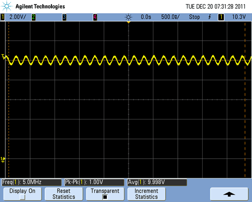
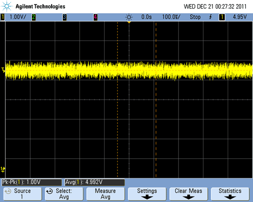
As an example, a TAMS circuit was implemented using an Agilent 33521A function/arbitrary waveform generator, an N6762A power supply, an E&I 1040L RF power amplifier, and 10-μF and 0.1-μF capacitors in parallel (for the coupling-capacitor section). A 1040L RF amp provided up to 400 W of output power, which was more than necessary, but that RF amp was what was readily available in the lab. Using the same load used in TOMS example, TAMS was used to create two noise signals: a 1-Vp-p, 5-MHz sine wave modulated onto a 10-Vdc level. and a 1-Vp-p, 5-MHz bandwidth Gaussian noise signal modulated onto a 5-Vdc level (see Fig. 4 ).


Fig. 4: Both the 1-Vp-p 5-MHz sine wave on 10-Vdc level (top) and the 1-Vp-p 5-MHz bandwidth Gaussian noise on 5-Vdc level (bottom) were generated by TAMS.
Instrumentation power supplies typically have a high capacitance value at their output. In TAMS, the power supply is in parallel with the load with regard to the RF amp’s output. That means the noise signal actually has two low-impedance paths to take: the load and the power supply’s output. It is hard to know the power supply’s ac power-handling characteristic across its input capacitance, since it is not specified by the power-supply manufacturer; so you may want to contact the manufacturer to avoid costly damage.
One safety precaution you can take is adding a blocking impedance between the power supply’s output and the coupling capacitor section. The blocking impedance can either be an inductor or a resistor. Its purpose is to protect the power supply from being damaged by the noise signal, which it does by adding higher series impedance before the power supply’s output. The inductor is ideal because it acts like a short to the Vdc from the power supply, but presents high impedance to the ac noise signal. However, the inductor can cause large oscillations on the dc level if the DUT has a very dynamic current.
Using a resistor, on the other hand, avoids the oscillations problem. Be sure to use the power supply’s sense leads to regulate the output voltage at the load to compensate for the voltage drop across the resistor. Also, be sure to use a low-value resistor, one no larger than 1 Ω. This is to ensure a low voltage drop across the resistor so you do not damage the sense lead circuit on the power supply. ■
Advertisement
Learn more about Keysight Technologies, Inc.


