Misbehaving electrical charge presents major hurdle for future computer chips
Designers will have to figure out solution if they intend to further develop technology
A recent report by a team of physicists at McGill University concluded that in order to build smaller yet still high-performing computer chips, designers will need to focus on better understanding how an electrical charge behaves when confined to metal wires only a few atoms thick.

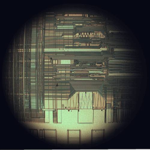
Upper interconnect layers on an Intel 80486 DX2 taken with an optical microscope at 200x magnification.
A very telling report
In collaboration with General Motors R&D, the McGill team published a new paper in Proceedings of the National Academy of Sciences that describes their investigation of an ultra-small contact between gold and tungsten, two metals that are currently used in computers chips to connect the different functional components of a device.
During experimentation, they used advanced microscopy techniques to image a tungsten probe and gold surface with atomic precision, bringing both metals together mechanically in a precisely controlled manner. They discovered that when they did this, the electrical current was much lower than expected.
The group found that crystal defects, that is, displacements of the normally perfect arrangement of atoms, generated by bringing the two materials into mechanical contact with one another was a reason for the reduction of current.
State-of-the-art electrical modeling by the research group confirmed this result. It also showed that dissimilarities in the electronic structure of two metals contributed to the fourfold decrease in current flow — even in instances when a perfect interface was used.
Reflecting on their discovery
McGill Physics professor Peter Grütter points out that they observed the resistance actually jumping around, displaying counterintuitive effects of quantum mechanics.
“You could use the analogy of a water hose,” he explains. “If you keep the water pressure constant, less water comes out as you reduce the diameter of the hose. But if you were to shrink the hose to the size of a straw just two or three atoms in diameter, the outflow would no longer decline at a rate proportional to the hose cross-sectional area; it would vary in a quantized (‘jumpy’) way.”
It’s an important discovery in this rapidly developing field of technology, especially as the size of features in electronic circuits continues to shrink year after year. “The size of that drop is far greater than most experts would expect — on the order of 10 times greater,” notes Prof. Grütter.
Outlook
Such a sharp reduction in current presents a major hurdle for designers of future computer chips as it will affect their choice in material along with the design of devices in the emerging field of nanoelectronics. Further research is now needed to look into ways to get around this problem, whether it’s to go with different materials or otherwise change current processing techniques.
“The first step toward finding a solution is being aware of the problem,” Grütter concludes. “This is the first time that it has been demonstrated that this is a major problem for nanoelectronic systems.” ■
Story via: mcgill.ca
Advertisement
Learn more about Electronic Products Magazine


