A look at Cortex-M0 and -M0+ microcontrollers

BY JIM HARRISON
The ARM Cortex-M0 and M0+ microcontroller core is one of the wondrous devices available to design engineers right now. It’s a 32-bit processing element in a small package at low cost. Chips using the M0 IP have been out for more than three years, and in the past year products with the M0+ core have arrived. Time to review some of the available versions.
The Cortex-M0 and -M0+ IP feature high code density and energy efficiency along with small die size (read: low cost). The M0+ has a two-stage pipeline, instead of the M0’s three stages — said to improve response time.
Tweaks to the M0+ yield even lower power and somewhat higher performance with a CoreMark/MHz of 1.77 (M0 is 1.62). It is said that, at least in some situations, the M0+ power is down 30% compared to an M0.
Both designs use the Nested Vectored Interrupt Controller (NVIC), which provides some advantages in real-time response, though interrupt response is still 16 cycles, under normal circumstances.
Companies selling this core target designs that have been done with 8- and 16-bit MCUs, and may have a good case. The cost is down around 50 cents in high quantity, they say the memory footprint is smaller than with an 8-bit, and they have made is easier to program. For one thing, with the M0+, it is possible to change the state of an I/O pin in one cycle — so bit-banging is easy.
Here are a few implementations:
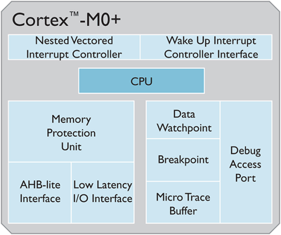
Fig. 1: The basic M0+ core from ARM.
The STMicrosemiconductor implementation of Cortex–M0
The STM32F050 and F051 family of MCUs combines a Cortex-M0 core with enhanced peripherals for sensing, control, and consumer devices. The devices operate from 2.0 to 3.6 V and have a 2.8-µ standby mode with the real-time clock running. Performance is said to be 0.9 DMIPS/MHz at up to 48 MHz.
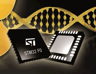
Fig. 2: The STM32F050 is available in a UFQFPN 32 package
The MCUs have 16 to 64 Kbytes of flash, a 12-bit 1-Msample/s A/D converter, a 12-bit D/A converter, and two analog comparators. They have a 4 to 32-MHz crystal oscillator and a 32-kHz oscillator, six PWM channels, I2 C, UART, and SPI interfaces, a RT clock/calendar, a 5-channel DMA controller, and a 96-bit unique ID. Going for $1.24 each in 1,000 qty, they are available right now.
Two NXP implementations
The Cortex-M0+ based LPC810M, LPC811M, and LPC812M microcontrollers from NXP are available in low-pin-count packages and offer easy-to-use peripherals addressing 8-bit application requirements with 32-bit Thumb instruction set. The chips feature a single-cycle multiplier and a fast single-cycle I/O port with 4 to 16 Kbytes of flash and 1 or 2 Kbytes of SRAM. I’m told they will cost as little as 39 cents when they are available in Q1.
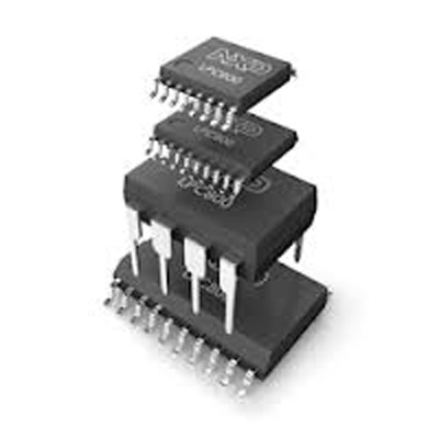
Fig. 3: Package variations from NXP.
The LPC81x takes simple API calls operate the ICs I2C and UART peripherals and power management is simplified to a single API call. 64-byte page flash simplifies code management and the chip has a 4-channel multi-rate timer, a wake-up timer, up to 18 GPIOs, a CRC engine, and a Micro Trace Buffer (MTB). The IC is available in SO20, TSSOP20, TSSOP16, and DIP8 packages and takes just 3 mA at 30 MHz and 3.3 V and 170 µA in deep-sleep mode. It’s one of the few MCUs I know of without an A/D converter.
Another NXP version features a flexible USB controller and a smart-card interface. The LPC11U12, LPC11U13, and LPC11U14 use the Cortex-M0. The chips’ Full Speed USB 2.0 device controller has up to 10 configurable physical endpoints.
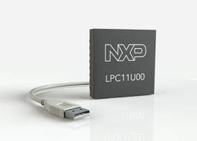
Fig. 4: The LPC11U12 provides USB conectivity.
USB endpoint buffers in the 11Uxx do not reside within the USB domain, like typical implementations, but in system SRAM, giving the CPU direct access to packets. This feature is especially suited for protocol converters such as UART-to-USB and SPI-to-USB bridges. Each non-control endpoint can be configured for either bulk, interrupt, or isochronous, and can be double buffered with maximum packet sizes of 1,023 bytes. The ICs come in a 4.5 x 4.5-mm TFGBGA48 package, operate from –40° to 85°C at 1.8 to 3.6 V, and have up to 32 Kbytes of flash, 6 Kbytes of SRAM, a variety of serial interfaces, four timers with PWM, and an eight-channel 10-bit A/D converter. They start at $1.44 in 1,000 quantity.
The Freescale KL series
The KL0 MCU family (Kl02, Kl04, Kl05) is the entry point into the Cortex-M0+ based KL Series. The 48 MHz chips feature a 12-bit A/D with ±1 LSB INL, 8-32K of 24 MHz flash, 16-bit PWM modules, and –40 to +105C operation. They take 142 µA/MHz max at 3.0 V in full-speed operation from flash with peripherals disabled and low power timer active.
Pin compatible with 8-bit S08P family, the Kinetis KL0x is a bridge to 32-bit design. Devices start from 8 Kbytes of flash in a small-footprint 4 x 4-mm 24 QFN package extending up to 32 Kbytes in a 48 LQFP package.
The Freescale Kinetis KL1 series offers up to 128 Kbytes program flash memory, up to 16 Kbytes RAM, 80-bit unique identification number, low-power hardware touch sensor interface, a 16-bit SAR A/D, and a bit manipulation engine. They take a very respectable 156 µA/MHz max in full operation from flash with peripherals disabled and low-power timer active.
The Kinetis KL2x adds a USB 2.0 port and flash up to 256 Kbytes. The KL3 series has a segment LCD controller, and the KL4 has both USB and LCD.
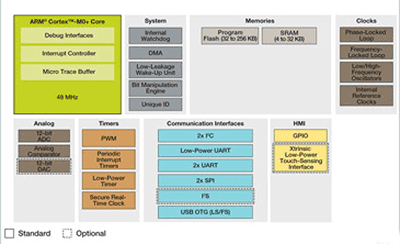
Fig. 5: The block diagram for Freescale’s Kinetis Kl2x processors.
NuMicro’s Cortex M0 offerings
The NuMicro NUC100, 120, 130, and 140 series with a Cortex-M0 core runs at up to 50 MHz with up to 512 Kbytes of flash, 64 Kbytes of SRAM, and a single-cycle 32-bit hardware multiplier. Options include USB, LIN, and CAN. Operating current is a rather high 28 ma at 50 MHZ and 3.3 V. The devices will operate at up to 5.5 V. The MCUs start at about $1.58 each in 1,000 quantity. Headquartered in Taiwan, Nuvoton’s U.S. office is in San Jose (408-544-1718).
Fujitsu FM0+ Family
Fujitsu has announced the FM0+ family of energy-efficient MCUs with a Cortex-M0+ core to be released in mid-2013. The chips have the features the peripheral functions of the FM3 family of Cortex-M3 MCUs. The FM0+ family targets an operating current of 70 μA/MHz and a standby current of just 0.7 μA (in RTC mode).
Advertisement
Learn more about Electronic Products Magazine


