Research done at Georgia Institute of Technology and at SOLEIL, the French national synchrotron facility, helped fabricate graphene structures atop nanometer-scale steps etched into silicon carbide (SiC). The investigators created an electronic bandgap in the material suitable for room-temperature electronics. Use of nanoscale topography to control the properties of graphene could facilitate fabrication of transistors and other devices, potentially opening the door for developing all-carbon integrated circuits.
The researchers measured a bandgap of approximately 0.5 eV in 1.4-nm bent sections of graphene nanoribbons. This development could provide new direction to the field of graphene electronics, which has struggled with the challenge of creating bandgap necessary for operation of electronic devices. This discovery will enable developers to design scalable fast transistors from graphene.
Currently, it is not understood why graphene nanoribbons become semiconductors as they bend into steps that are cut into the silicon carbide wafers, but the researchers believe that strain induced as the carbon lattice bends and the confinement of electrons may be factors creating the bandgap. These nanoribbons are composed of two layers of graphene.

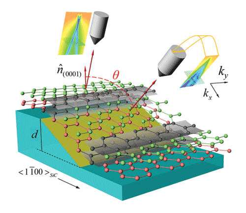
This diagram shows the experimental geometry of measuring graphene in silicon carbide trenches. The research showed a substantial electronic bandgap in the material.
Production of the semiconducting graphene structures begins with the use of e-beams to cut trenches into silicon carbide wafers, which are normally polished to create a flat surface for the growth of epitaxial graphene. Using a high-temperature furnace, tens of thousands of graphene ribbons are then grown across the steps using photolithography.
During the growth, the sharp edges of the trenches become smoother as the material attempts to regain its flat surface. The growth time is carefully controlled to prevent the narrow SiC features from melting too much. The graphene fabrication also must be controlled along a specific direction so that the carbon atom lattice grows into the steps along the material’s armchair direction. The new technique permits creation of a bandgap in the material, and also the fabrication of entire integrated circuits from graphene without the need for interfaces that introduce resistance. On either side of the semiconducting section of the graphene, the nanoribbons retain their metallic properties.
By growing the graphene down one edge of the trench and then up the other side, the researchers could in theory produce two connected Shottky barriers – a fundamental component of semiconductor devices.
Confirmation of the bandgap came from angle-resolved photoemission spectroscopy measurements made at the Synchrotron CNRS in France. There, the researchers fired powerful photon beams into arrays of the graphene nanoribbons and measured the electrons emitted. Theorists had predicted that bending graphene would create a bandgap in the material. But the bandgap measured by the research team was larger than what had been predicted.
Beyond building transistors and other devices, in future work the researchers will attempt to learn more about what creates the bandgap — and how to control it. The property may be controlled by the angle of the bend in the graphene nanoribbon, which can be controlled by altering the depth of the step. Find more information at http://gtresearchnews.gatech.edu/semiconducting-graphene-patterned-silicon-carbide/.
Paul O’Shea
Advertisement
Learn more about Electronic Products Magazine


