PCI Express (PCIe) has become the most popular interface for chip-chip and board-board communications in PC and embedded applications. PCIe is a point-point, multi-lane, serial-bus architecture that can run up to 8 gigatransfers/s for each PCIe (third-generation) lane. These high-speed serial lines impose demanding jitter requirements on the reference clocks, along with a multi-clock capability to support the PCI Express Transmit / Receive physical layer. A new generation of MEMS clock generators is ideally suited to meet this application.
The Peripheral Component Interconnect Special Interest Group (PCI-SIG) is the organization that develops the PCIe specifications to ensure that devices from all vendors are interoperable. The PCI Express architecture is a point-to-point serial link containing both clock and data sharing the same physical connection. Placing clock and data together on a serial line eliminates problems associated with timing skews seen in parallel data bus designs, creates a scalable method to increase clock and data rates, and reduces complexity. At present, there are three levels of PCIe: PCIe Gen 1 (2.5 Gbytes/s); PCIe Gen 2 (5.0 Gbytes/s); and PCIe Gen 3 (8.0 Gbytes/s). All three standards are sourced from a 100-MHz reference clock, but the jitter requirements become increasingly more difficult to meet as the PCIe data transfer rates increase.

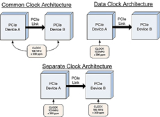
Fig. 1: The PCI-SIG specifies three clock architectures for PCIe links — all of which use a 100-MHz, ±300-ppm reference clock.
The PCI-SIG specifies three clock architectures for PCIe links — all of which use a 100-MHz, ±300-ppm reference clock (see Fig. 1 ). The PCIe link is made of a transmitter (Device A) and a receiver (Device B). The Common Clock Architecture uses a single reference clock to source Device A and Device B. The Data Clock Architecture sources Device A with a reference clock, but Device B must recover the clock from the serial Clock/Data stream. The third configuration, the Separate Clock Architecture, provides Device A and Device B with independent reference clocks. For each PCIe generation and clock architecture, the PCI-SIG has standardized transfer functions for the Transmit PLL, the Receive PLL, and the Clock Data Recovery block. For many of these filtering functions there are multiple bandwidths and peaking values that must be considered to compute all permutations. PCIe Gen 3 Common Clock Architecture has 32 such transfer function combinations.
Clock Generator devices vary in capability to meet these jitter requirements. One major vendor has three dual-clock solutions, each targeted for a particular PCIe Generation level of performance. Gen 1-, 1.1 -,and 2.1-capable devices are available in a 5.0 x 6.4-mm 16-pin TSSOP package and a Gen 1.1-, 2.1-, and 3.0-capable device is available in a smaller 4 x 4-mm package. The newer devices use a smaller lithography, and the maximum voltage is lowered from 7.0 to 4.6 V, or to 2.5 V with the latest devices. Each of these requires an external crystal resonator and the associated headaches of tuning crystal center frequency on a PCB during production.
Other available devices use a new generation of MEMS-based resonator in a dual-output clock generator that meets the PCIe Gen 1.1, 2.1, and 3.0 jitter requirements. These devices are available in a 16-pin TSSOP, which can drop into existing designs, or the more compact 14-pin 3.2 x 2.5-mm QFN package. The MEMS resonator is in the same package as the CMOS ASIC and, since the frequency is set at the factory, tuning is not required during production. The outputs are not limited to HCSL, but are also available in LVDS, LVPECL, and LV CMOS at 2.5 and 3.3 V.
PCIe is a point-to-point serial link and many designs have multiple PCIe links between bridges, switches, solid state memory, and other peripheral devices. There are three and four output clock generators available in a 5.0 x 3.2-mm, 20 QFN plastic package.

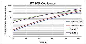
Fig. 2: A population of >5.6 million units will have a failure rate of
These advanced devices also feature an internal fractional-n phase lock loop for multiple outputs. While not every combination of frequencies is available from this architecture, the important frequencies in today's products can be generated. MEMS technology provides reduced cost and reduced PCB area, along with increased reliability over a crystal resonator. Depending on the system lifetime operating temperature, MEMS can have a 20-times-lower failure rate, compared to quartz. The reason is the activation energy to failure for crystal SiO2 (0.4 eV) vs. MEMS SiO (0.7 eV). The chart to the right shows the mean time to failure (MTTF), comparing Discera MEMS oscillators to industry-standard crystal oscillators. Figure 2 shows a population of >5.6 million units that will have a failure rate of
The PCIe reference clock requirements are varied and complex, fortunately the hard work has been completed to confirm that the clock generator devices meet or exceed these numerous jitter requirements. The DSC557-03 from Discera (www.discera.com) is an example of a high-performance MEMS-based clock generator that is available right now. And, the family provides two, three, or four outputs.
Advertisement
Learn more about Discera


