BY MATT APANIUS, Director
Desich SMART Microsystems Center
www.smartmicrosystems.com
ROGER H. GRACE
President
Roger Grace Associates, www.rgrace.com
and LELAND “CHIP” SPANGLER, Ph.D., Aspen Microsystems
aspenmicrosystems.com
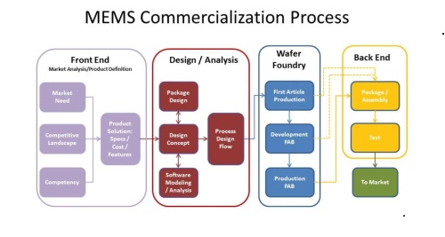
The role of packaging/assembly/test (P/A/T) in the overall successful commercialization of MEMS (microelectromechanical systems) has historically taken a backseat to device development. In the beginning, MEMS were virtually stand-alone devices inserted into custom-designed mechanical enclosures or standard IC packages, and tested in an ad hoc manner. Now, MEMS are truly becoming systems (as the “S” in MEMS connotes). MEMS devices are being integrated into packages of various shapes, sizes, and materials, along with signal-conditioning electronics, power sources, and communication network (both wireless and connected) ICs are to make MEMS into complete application solution (see Fig. 1 ). As this occurs, the MEMS community is taking note of the importance and the value of P/A/T in the creation of MEMS-based solutions.

Fig. 1: While much effort has been expended on development of front-end, design/analysis, and wafer-foundry requirements for MEMS commercialization, back-end process creation has not received the serious attention required to make MEMS manufacturing truly mainstream.
Additionally, it is well known that the packaging/assembly and test (P/A/T) of a MEMS-based solution can be as much as 60% or more of the total cost of the solution. This fact makes the consideration of the packaging strategy a very important and early part of the solution design process to achieve optimum cost and performance. Here we are, almost a half-century later from the early days of MEMS packaging, yet many of the same materials and packaging strategies are still favored by many suppliers.
Packaging challenges
The requirements for MEMS packaging are fundamentally different than those for ICs, although IC package assembly technology is at the foundation of most MEMS package assembly processes. The differences between MEMS and IC packages revolve around two fundamental topics: interface to the real world, and sensitivity to stress.
Because the majority of MEMS devices are intended to sensing real-word phenomena, a MEMS package must interface with the outside world. The desired optical, mechanical, magnetic and/or chemical signals must have a path to connect to the MEMS microfabricated die. At the same time, the package must also protect the die from undesired and possibly damaging forces from the outside world, while also providing electrical signal and power connections. Managing this interface so that desired signals are transferred to the die with minimum noise or attenuation is one of the most challenging and costly facets of MEMS packaging.
The second major difference in MEMS vs. IC packaging revolves around MEMS die often being much more sensitive to stress then ICs. This stress primarily results from differences in the temperature coefficients of the materials that make up the MEMS device and its package. This difference in temperature coefficients and the die stress that results usually leads to a temperature coefficient in the device bias and scale factor output. While this temperature sensitivity can be compensated for in the interface electronics, it, along with the associated calibration process, adds significant cost. Furthermore, if not properly designed, these temperature coefficient differences can change over time, resulting in a device that no longer operates to specification or, in extreme cases, fails.
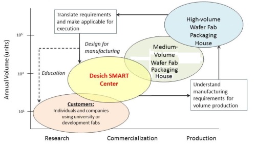
Richard Desich SMART Commercialization Center for Microsystems (“Desich SMART Center,” or DSMC) provides a unique means to develop appropriate technologies for P/A/T without having to risk substantial capital while at the same time having access to the top equipment and technologies. (See side bar.) The ultimate commercialization role of DSMC is to provide a developmental P/A/T “bridge” between the suppliers of MEMS wafers and the high-volume MEMS packaging suppliers (see Fig. 2). Prior to the availability of the Center, this function was virtually nonexistent in the MEMS community, seriously disrupting timely and cost-effective commercialization. (The need for such a service, its targeted customers, and the details of its offerings were determined through an in-depth market research study conducted for the Center by Roger Grace Associates.)

Fig. 2: The DMSC aims to provide a closed-loop information process for seamless MEMS manufacturing transitions.
The DSMC is centered about a core facility with end-to-end microsystem packaging and assembly capability supported by reliability test equipment and further augmented by software design tools and materials databases. Such a complete packaging capability promotes efficient problem-solving in what is typically a multistep, iterative process. A single facility to investigate and prototype manufacturing processes for microelectronic packaging facilitates product codesign, and reduces the risk of contamination and damage due to shipping to job shop vendors; it streamlines project time frames, communication, and error causality tracking. The primary objective of the facility is to determine a package design for a specific product application, providing a resource for down selecting options from current manufacturable processes as a customer weighs this against product cost and supply chain limitations.
DSMC is currently located in a temporary 1,800-sq ft class 10,000 cleanroom in the Entrepreneurship Innovation Center (EIC) on Lorain County Community College’s campus while a new, three-story, 47,000-sq ft facility being built adjacent to the EIC building. The first floor of the new facility, scheduled for completion by the third quarter, 2013, will house state-of-the-market laboratory space, including class 1000 and class 100 cleanrooms. The equipment configuration establishes the facility as a “pilot plant” for manufacturing, thus facilitating the ease of transition from lab to manufacturing environment. The second floor is reserved for incubating startup companies, as well as corporate incubating space to allow larger corporations a secure environment to innovate new product developments. The third floor will house the computer lab with software design tools, as well as wet labs that are available for rent.
Case/application studies
It is important to understand the potential trade-offs when a device transitions from the “proof of concept” prototype to a “production intent” design. DSMC has supported numerous customers with this transition by increasing performance and yield with die-to-package interconnects. The replacement of hand soldered connections with aluminum wedge bonding may seem remedial but is not unusual. More complex scenarios, such as gold ball bonding on thermally isolated die mounted in TO headers or pin dip connections on two-sided custom assemblies, required engineering development before the solution was delivered to the customer.
Since packaging solutions tend to be complex in nature, the Desich SMART Center works very closely with the customer to ensure that the development pathway is aligned with existing designs and suppliers. Parylene and silicone are materials used to encapsulate sensor devices in ambient and liquid environments. In one case, deposition experiments were run to examine mechanical robustness versus degradation of sensor performance. This work provided actionable data for the customer to update a specification back to their supplier.
In another situation, reliability tests such as HAST, thermal-humidity cycling, high temperature storage, and biased 85/85, were conducted to qualify the design of a commercially available MEMS assembly for an end user. Here an encapsulation material specified for one environment was being qualified for a more stringent environment. The qualification allowed the customer to move their program into the next phase of product development.
A “production intent” design permits customers to sample their product while they work their strategy for volume production. Relying on offshore volume packaging houses for package assembly development and “proof of concept” prototypes is often very inefficient. Using wafers from small custom lots or shuttle services, DSMCoffers “on demand” prototypes. In one example, process development was required for the assembly of high temperature devices using standard ceramic packages. The development was necessary to address the novel high temperature materials and multiple designs used on the wafer. The turnaround time with the current process is one day.
SIDEBAR
Desich SMART Center
With the recent availability of the Richard Desich SMART Commercialization Center for Microsystems (“Desich SMART Center,” or DSMC)), the MEMS community now has a viable resource to overcome package, assembly and, test-based barriers to full commercialization. The DSMC not only provides critically needed resources to the MEMS community, but also serves as the core of the emerging Northeast Ohio Microsystems Technology Cluster.

DSMC is developing relationships using a web-like structure with other organization in the area that provide complimentary services to the microelectronics community. The cluster’s primary role in the local community is to be an economic engine for creating high paying manufacturing jobs for regional citizens, many of whom have been displaced by the closing of the numerous manufacturing plants that once populated the area.
Technically speaking, the DSMC is a microsystem packaging, assembly, and test development foundry. Located on the campus and a part of Lorain County Community College in Elyria, OH, DSMC develops manufacturable packaging integration technologies for customers developing next-generation microsystem products. It does so by leveraging world-class facilities and a highly experienced engineering team to accelerate product time to market.
DSMC is currently located in a temporary 1,800-sq ft class 10,000 cleanroom in the Entrepreneurship Innovation Center (EIC) on Lorain County Community College’s campus while a new, three-story, 47,000-sq ft facility being built adjacent to the EIC building, as seen in the above photo. The first floor of the new facility, scheduled for completion by the third quarter, 2013, will house state-of-the-market laboratory space, including class 1000 and class 100 cleanrooms. The equipment configuration establishes the facility as a “pilot plant” for manufacturing, thus facilitating the ease of transition from lab to manufacturing environment. The second floor is reserved for incubating startup companies, as well as corporate incubating space to allow larger corporations a secure environment to innovate new product developments. The third floor will house the computer lab with software design tools, as well as wet labs that are available for rent.
Advertisement
Learn more about Roger Grace Associates


