Analog signature analysis (ASA, also known as V-I testing) is an elegant, powerful fault-diagnosis technique for printed circuit boards, and is the method of choice whenever circuit diagrams and documentation are lacking. In these situations, comparative analog signature analysis can be used by matching the analog signatures of a known-good printed-circuit assembly with those of a suspect one; signature differences can indicate a potential problem. A major advantage when testing a board with a V-I tester is that the device under test doesn't need to be powered up. This makes the technique ideal for evaluating so-called “dead boards.”
With V-I testing, a precision current-limited sine wave signal is applied to appropriate points or components on the device under test using touch-probes, and the resulting current flow, voltage drop, and signal phase shift (that is, the characteristic impedance) is displayed by plotting voltage against current on a monitor. The current flow is displayed as a vertical trace deflection on the display, while the voltage across the component is shown as a horizontal trace deflection (X axis = voltage; Y axis = current). The resultant trace on the display is called the “analog signature.”
For V-I testing, a stimulus waveform, usually a sine wave, is applied through a current-limiting resistor across the device under test (Fig. 1 ). The voltage across the device under test (DUT) is plotted on the display's horizontal axis against the current through it shown on the display's vertical axis. Each test signal or range has four basic parameters: source waveform and voltage (Vs ), source impedance (Rs ), and source frequency (Fs ), varied to yield descriptive and revealing analog signature at various test points.
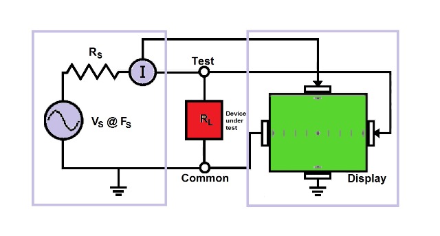
Fig. 1: For capturing analog signatures, a V-I tester with a variable-frequency and -voltage signal source, current measurement, and display are required. The voltage drop across the device under test (DUT) drives the display in the x axis, while the measured current through the DUT drives the display's y axis.
From Ohms' law (R = V/I), it can be seen that the resulting characteristic represents the impedance of the DUT.Impedance is frequency related for frequency-dependent components such as capacitors and inductors, so a variable-frequency stimulus is required for these types of components. The current-limiting resistor Rs and the DUT form a voltage divider, so to achieve a usable trace, the current-sense resistor should be the same order of magnitude as the impedance of the DUT at the test frequency. Thus, to use this technique on a wide range of DUTs, a wide range of current-limiting resistors is required.
In real-world board-fault-diagnosis situations, several components may be connected to a particular node, and the resulting analog V-I characteristic will be a complex composite of the individual components' characteristics, making it somewhat difficult to completely understand. However, most applications employ analog V-I testing in a comparative manner, where understanding the displayed characteristic is not necessary. Contrasting the signatures of one “good” board with another under test is all that is needed.
Understanding the display
The V-I display plots the voltage across the device under test (V) on the horizontal axis, and the current through the device under test (I) on the vertical axis. Different types of components and devices produce different signatures, depending on the current flow as the applied voltage changes, with four basic Component Analog Signatures: resistance, capacitance, inductance, and semiconductance (Fig. 2 ). Each of these four fundamental components responds differently to the sine-wave test signal. Recognizing these four basic unique signatures on the instrument display is one of the keys to successful ASA troubleshooting.
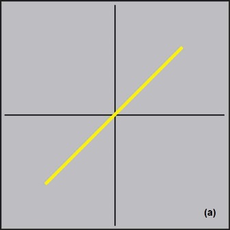
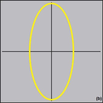
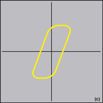
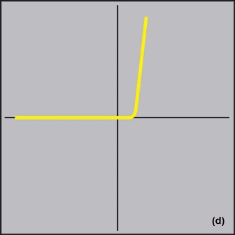
Fig. 2: The analog signatures shown here for resistance (a), capacitance (b), inductance (c), and semiconductance (d) show typical shapes. Actual shapes may vary, but having an analog signature for a device onknown-good board lets users compare the shape of the DUT's analog signature to see if there is a deviation indicative of a fault.
The actual signature at a circuit node is a composite of the basic component signatures at that point in the circuit. For example, a circuit with both resistance and capacitance will have a signature that combines the analog signatures of both a resistor and capacitor.
Shorts/Opens
The majority of faults on failed boards are gross failures such as short or open circuits, and are easy to detect with the V-I technique without complex analysis. A short circuit (0-Ω resistance) would be displayed as a vertical line, because the current flow for any applied voltage would be theoretically infinite, whereas an open circuit (infinite resistance) would display a horizontal line because the current is always zero irrespective of the applied voltage (see Fig. 3 ).
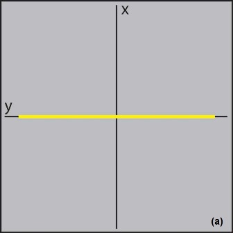
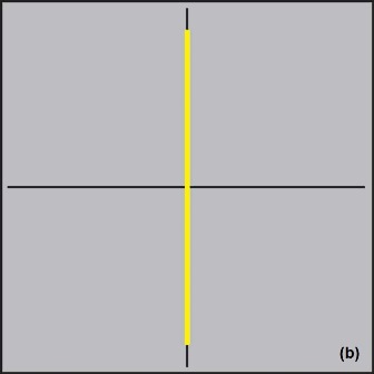
Fig. 3: Analog signatures for shorts (a) and opens (b) vary in only one axis.
Resistors, capacitors, and inductors
The signature of a resistor is indicated by a straight line at an angle from 0º to 90º, whose slope depends on the resistance, as current is proportional to the applied voltage (Fig. 4a ). The higher the value of the resistor under test, the closer the line gets to the horizontal (open circuit). For best accuracy, the source impedance of the V-I tester should be selected so the slope of the line, for a good resistor, is close to 45º. A difference in the slope of the curve when comparing a good and suspect board indicates a difference in the resistor values on the two boards.
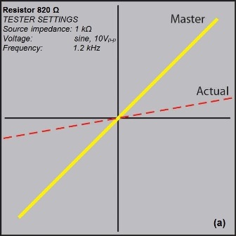
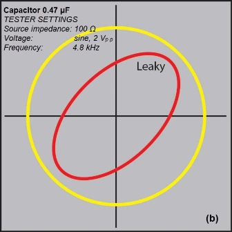
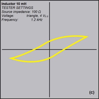
Fig. 4: The analog signatures shown here for a resistor (a), capacitor (b), and inductor (c) indicate how faulty components differ from know good ones.
The signature of a capacitor is an approximate circle or ellipse (Fig. 4b ). Capacitors with relatively low values have flattened, horizontal, elliptical signatures, and capacitors with relatively high values have flattened, vertical, elliptical signatures. The optimal signature is a nearly perfect circle, which can be obtained by selecting the appropriate test frequency and source impedance. Typically, the higher the capacitance, the lower the test impedance and frequency. A leaky capacitor would give a sloping curve due to the effective resistance in parallel with the capacitor.
The signature of an inductor is circular or somewhat elliptical due to internal resistance, and may show hysteresis (Fig. 4c ). Inductors with relatively high values have flattened, horizontal, elliptical signatures similar to those of capacitors. The optimal signal is a perfect circle. Inductors may have ferrite, iron, brass, or air cores, which may or may not be adjustable. Inductors with the same value may have very different signatures if they use different core materials or if the core is positioned differently. Inductors usually require a low source impedance and higher test frequencies to exhibit an elliptical signature.
An open-circuit inductor (a common fault with small PCB mounting devices) can easily be detected by the noticeably different V-I curves when comparing two boards.
Semiconductors
A semiconductor diode signature is made up of two or more linear line segments that resemble a right angle, with conduction in both forward- and reverse-bias. The signature of a silicon diode can be identified easily (Fig. 5a ). The vertical part of the curve shows the forward bias region, and the turn-on voltage and the forward voltage drop can be easily identified. The curved area of the trace shows the changeover from fully off to fully on as the applied voltage increases. The horizontal part of the curve is the reverse voltage region where the diode is non-conducting and is effectively an open-circuit. Faulty diodes can easily be identified by a deviation from this characteristic; for example, a diode which exhibits significant reverse leakage would have a diagonal curve in the reverse region, similar to a resistor.
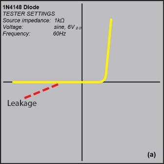
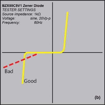
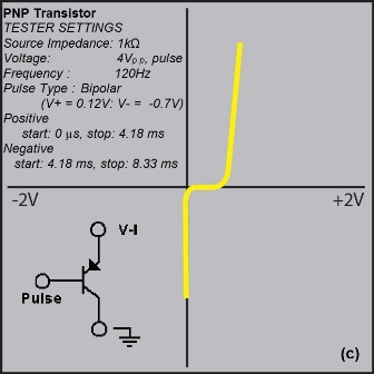
Fig.5: In (a), the analog signature for an ordinary diode can indicate leakage, while that for a zener diode (b) can indicate bad cut off or leakage. For a pnp-type transistor, use of a pulsed bias voltage at the transistors base will allow meaurement of its operating characteristics.
Zener diodes conduct in both directions. The forward current characteristic is similar to that for a diode, while the characteristic in the reverse direction is also similar to a diode until the breakdown or Zener voltage is reached, at which point the current increases rapidly and the diode voltage is clamped. This yields the curve in Fig. 5b . The test voltage should be chosen to be higher than the Zener voltage for this curve to be obtained. A suspect Zener diode may not have a well-defined “knee” and the horizontal part of the curve in the reverse region may exhibit leakage effects in a similar way to a normal diode.
NPN and PNP bipolar transistors have a signature similar to that of the diode when tested between the base-collector and base-emitter junctions. If tested between the collector-emitter terminals, the signature would appear to be an open circuit. A pulse generator can be used to apply a bias voltage, via a suitable resistor, to the base of the transistor, so that the switching action can be observed (Fig. 5c ). The pulse generator can also be used to trigger devices such as triacs and thyristors to test switching action. Transistors with open-circuit or leaky junctions can easily be identified by the marked differences between curves.
Advertisement
Learn more about Saelig


