Figure 1
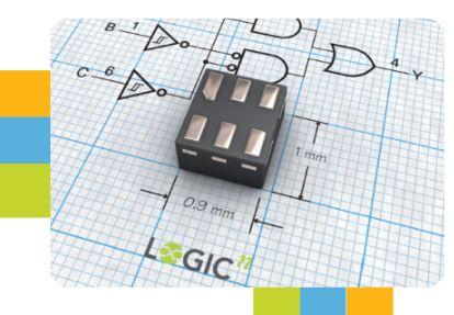
“The mobility markets have been exploding in recent years,” NXP's International Product Manager, Cliff Lloyd told us. “That market is driven by two primary factors: one is the size of a device, and the other is battery life.” In the past, he explained, NXP focused on making smaller and smaller packages. NXP made a breakthrough last year in small package size when it released its Diamond package – 0.8 by 0.8 in size with a 0.5mm pad pitch – which made it easier to mount on PCBs. After the Diamond package was released and package size addressed, NXP decided to focus on addressing low power consumption in the mobility market. “We felt we had to address the need for faster performance… and also maintain or improve power savings performance,” said Lloyd.

Figure 2
There are two very important parts to power savings performance, explained Lloyd. The first is static power consumption, which is the amount of power a device uses when it is simply connected to a battery. The other important part of power consumption is the power that's consumed when the device is actually being used, which is called the Dynamic Power Consumption.

Figure 3
Keeping these two parts of power consumption low was what NXP has aimed to address with the AXP family. What they have achieved with the AXP family is 15% lower power consumption for unique functions, as well as a top delay of 4 nanoseconds at 1.2V, which is about twice as fast as its previous AUP family at the same voltage node.
One of the advantages of the AXP family of devices is its configurable logic, which gives customers a lot of flexibility when selecting parts. For instance, when a customer buys a device – depending on how he hardwires it on the PCB – the device could operate as a NAND Gate, an OR Gate, a NOR Gate, a buffer, or an inverter, and the customer doesn't have to buy a different device to perform these individual functions. The customer can get different functions from one device, and use a single qualification to cover multiple functions, which offers tremendous flexibility.

Figure 4

Figure 5
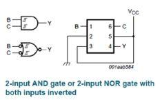
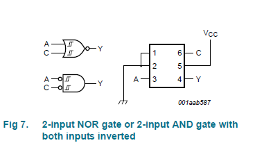
Although many people believe that the devices are programmable, Lloyd explained that that is a misconception. The devices are strictly hardwire configurable on the PCB. For example, if you hooked up pin 5 and pin 3, as in the figure 6 below, you would get a two- input AND gate. If you connected pin 2 and pin 1 to ground, you would get a two-input NOR gate as shown in figure 7. It all depends on how the board is laid out – an inverter, or an exclusive NOR (XNOR) can also be achieved. Because of this flexibility, NXP decided to first release the configurable devices.


Figure 6 Figure 7
With low static and dynamic power dissipation, a wide voltage range, true Schmitt-Trigger inputs, and configurable logic, NXP has aimed to address the need for low power consumption and reliable logic level switching with the AXP Logic family, and position itself for a mobile market where battery critical applications and battery life conservation is key.
Advertisement
Learn more about NXP Semiconductors


