Within the first week of debut, the LOGi-family of FPGA development boards has surpassed its Kickstarter crowd-funding goal by four times the amount. The popular boards simplify embedded systems development and unite FPGAs with the hardware interfaces of popular open-source ARM development platforms, without requiring custom port interfaces or proprietary programming hardware.
Why FPGAs
Short for field-programmable gate array, the FPGA is a programmable logic device that converts low level code written in a hardware descriptive language (HDL), such as VHDL or Verilog, into a dedicated logic-circuit that’s capable of processing data in a highly efficient manner. This is because the series of logic-gates, converted from the low level code, communicate directly in the machine-language, thereby, bypassing the need for a compiler. As a result, data will be processed in a parallel fashion and create stronger power/performance ratios than result from high level code being converted into machine-language using a processor.

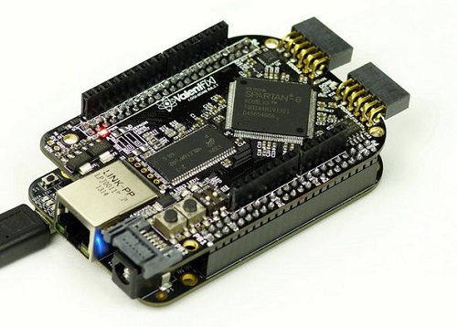
The FPGA converts code into connected logic-gates to form specialized chips. Seen above is the LOGi bone for the Beaglebone Black.
The ability to create hardware using an FPGA grants paramount flexibility; by determining function at runtime and assigning the number of serial ports and input or output pins, users can effectively repurpose a single FPGA board to match the changing needs of the project.
Nevertheless, the FPGA is not accessible to the everyday hobbyist as it requires specific knowledge of HDL and is awkward to interface with. Valent F(x), the makers of the LOGi boards, seek to remedy this issue by enabling users to program their LOGi-board through their favorite development platform: Raspberry Pi, Beaglebone Black, or Arduino DUE. Additionally, all LOGi-boards include a JTAG header to permit interfacing with a JTAG programmer or to use the FPGA board as a standalone device.
Tech specs
Presently, the LOGi-board is available in two varieties: the LOGi-Pi and the LOGi-Bone. Valent F(x) assures us [in their Kickstarter campaign] that the Arduino UNO specific LOGi board is under development.
LOGi boards were designed to promote quick plug-and-play, making it extremely easy to link with the Pi and Beaglebone. The Pi variant has a connector on the bottom to interface with the Raspberry Pi’s GPIO header. Similarly, the LOGi-Bone is the FPGA of choice for the Beaglebone enthusiasts; two rows of connectors are included on the underside of the FPGA board to interface with the 2×46-pin headers on the Beaglebone Black. Regardless of selection, all LOGi boards come equipped with the Xilinx Spartan 6 FPGA, a capable FPGA that delivers an optimal balance of low risk, low cost, and low power, with up to 150K logic cells.
LOGi-Bone Features:
• Xilinx Spartan 6 LX9 TQFP-144 FPGA 9,152 Logic Cells, 16 DSP48A1 Slices, 576KB Ram, and 96 User Available I/O Pins
• Beaglebone Black Optimized 4 Layer Optimized Design to Support Maximum Performance of High Bandwidth Applications Length-tuned GPMC, SDRAM, LVDS Signals 3.3v I/O Regulator and 1.2v Core
• Regulator 256 Mb SDRAM connected to the FPGA
• 2x LEDs 2x Push Buttons 2x DIP Switches
• 1x High Bandwidth SATA connector expansion port Length tuned and impedance routed differential signals for maximum bandwidth
• 2x Digilent Inc. PMOD ports supporting 59+ plug-and-play hardware modules
• 1x Arduino compatible headers connected to the FPGA pins (3.3v only) Supports over 200+ Arduino Shield Modules
• Optional GPMC, SPI or I2C port access from the Beaglebone Black
• 10x Length-tuned LVDS Pairs
• Bit-Stream loading interface connected to the host processor, optional bitstream FPGA self-loading from onboard Flash.
LOGi-Pi Specific Features
• Xilinx Spartan 6 LX9 FPGA 9,152 Logic Cells, 16 DSP48A1 Slices, 576KB Ram, and 96 User Available I/O Pins
• Plug-and-Play Interfacing for the Raspberry Pi 4 Layer Optimized Design to Support Maximum Performance of High Bandwidth Applications Length-tuned GPMC, SDRAM, LVDS Signals
• 3.3v I/O Regulator and 1.2v Core Regulator
• 256 Mb SDRAM connected to the FPGA
• 2x LEDs 2x Push Buttons 2x DIP Switches
• 1x High Bandwidth SATA connector expansion port Length tuned and impedance routed differential signals for maximum bandwidth
• 2x Digilent Inc. PMOD ports supporting 59+ plug-and-play hardware modules
• 1x Arduino compatible headers connected to the FPGA pins (3.3v only) Supports over 200+ Arduino Shield Modules
• 10x Length-tuned LVDS Pairs 32 FPGA I/O available through PMOD and Arduino headers
• Connection to the SPI Interface of the Raspberry Pi (3.8 MBps maximum Bandwidth)
• Connection to 16 I/O of the Raspberry Pi expansion port (including SPI, UART, I2C and GCLK and GPIO).
• Bit-Stream loading interface connected to the host processor, optional bitstream FPGA self-loading from onboard Flash.
Project ideas
If you’re aching to put your LOGi-board to work straightaway, Valent F(x) provides a series of demos based on the LOGi-Hardware library that users can download, load, and run without the need for any design and debug time. 
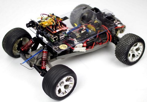
These include the autonomous vehicle control demo which provides all the material needed to start building your own AGV, a bitcoin-mining demo that autonomously mines bitcoins while you chill, a machine vision demo, and a LED message blinking demo.
Visit LOGi’s Kickstarter page to secure your own FPGA.
Advertisement
Learn more about Electronic Products Magazine


