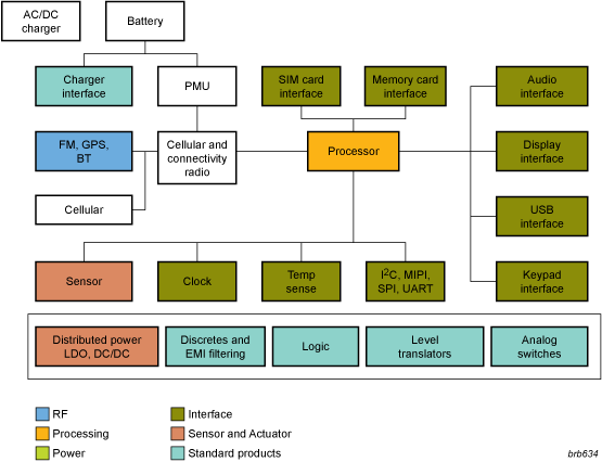
NXP recognizes that portable navigation devices face a number of challenges, such as short GPS times to first fix in urban environments. In addition, NXP looks to reduce filter losses caused by multiple frequencies and band jamming signals, which can decrease GPS receiver sensitivity. Another priority is quality, and NXP has the ability to enable clear and loud sound in a noisy environment. Finally, we aim to provide optimized application specific solutions, which includes protection from ESD charges at a system level.
Memory Card Interfaces
According the IEC61000-4-2 standard, SD host interfaces require additional high-level ESD protection, in addition to the integrated ESD protection which is typically very weak. Other strict EMI regulations and system requirements, as specified in GSM mobile phones, strongly request filters that reduce the radiated/conducted EMI. However, they must still comply with the electrical requirements of the interface specification.
The continuing trend of miniaturization of portable appliances implies that interface devices offering ESD protection and EMI filtering should also integrate biasing circuits/resistors into a single small-sized package. NXP’s memory card interface solutions fully support this continuing trend and offer interface conditioning functions such as high-level ESD protection according the IEC61000-4-2 standard. They also support EMI filtering, integrated biasing resistor networks, regulated power supply to supply SD-memory cards directly from a battery, and voltage level translation to enable the use of low-voltage host processors to communicate with 2.7 V to 3.6 V compliant SD-memory card devices.
GPS LNA
There is an increase in multiple RF frequency and RF system integration into portable appliances at the request of the consumers. The need for higher performance requires maximum sensitivity from receiver antennas without being disturbed by jammers and other disturbances from different RF systems. NXP’s LNA require an industry minimum in external components, while offering a top noise and jammer suppression performance.
Housed in an extremely small package, NXPs latest LNA requires only one external matching inductor and one external decoupling capacitor. It adapts itself to the changing environment in response to the presence of different radio systems.
Charger interface
Whether your device is charged via the USB port or a separate charger, it is exposed to incorrect polarity or abnormally high voltages. Any of these two occurrences poses a threat to the charger circuit and the PMU of the mobile device. In addition, the USB/charger port can be subject to ESD strikes and other transient discharges.
NXP offers an application specific portfolio of TVS diodes and ESD arrays, which enable cost efficient protection solutions – ESD, reverse polarity, overvoltage, other transient discharges – with the smallest footprint.
Audio
Our digital audio amplifier family is built to simplify audio architecture by lowering the system cost and enabling easy interfacing. Using a digital interface eliminates the need for a D/A converter in the host processor, and the PDM or I2S format guarantees an ultra small IC footprint.
The digital interface assures low RF susceptibility in the device and the total system, and low sensitivity to input clock jitter. In addition, the digital interface eliminates the need for couple capacitors and safeguard speakers by eliminating problems coming from DC offsets due to leakage currents of an analog design.
Click here for brochure
Download Full Block Diagram Below
Advertisement

Learn more about NXP Semiconductors


