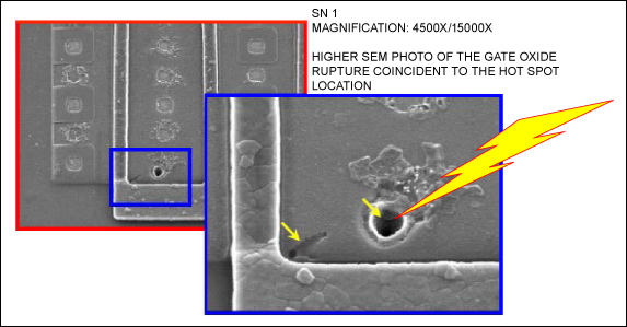
You are 15 times more likely to be struck by lightning than to win a lottery jackpot in the United States. Worse yet, being struck by lighting is a one-in-a-million chance given there were only 280 reported instances during the last decade, compared to nation’s population of 310,000,000 people. However, miniature lightning bolts caused by friction are far more common events, and while these sparks usually do no more than deliver a slight painful sensation, they can wreck complete and utter havoc on ICs and FPGAs.
When two objects come into contact, rub, and are separated, a trace amount of electrons transfer between the two, causing electrostatic discharge; the amount of electrons moved depends on the materials surface. This phenomenon, called triboelectric charge, is actually quite common considering most materials, insulators, and conductors exhibit triboelectric properties. Protecting FPGAs and ICs against ESD is a matter of adopting analogous parts with bigger geometries to compliment the FPGA’s smaller geometries.

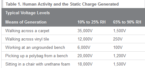
Differing actions create differing amount of electrostatic discharge.
That static shock you feel when touching a door knob after walking across a carpet? Yup, that’s triboelectric charge at work. If 5,000 volts can jump 0.4 inch in 50% RH air and create a pain in a five to six foot human, just consider the dire consequences wrought on to something that’s a few micro-inches tall, like an integrated circuit or transistor. To put this size difference in a more relatable perspective, consider that in 2012, a typical transistors measured 28 nm in size; this allowed semiconductor’s to pack as many as 6.8 billion in a single manufactured CPU chip. So how does one protect such miniature geometry against ESD?

Sources of board-level ESD problems
Solution 1: employ ESD protection circuitry
Using analog mixed-signal ICs that bridge the digital and analog realm is the one solution against ESD. ICs of this nature are far more robust and ESD-tolerant than their digital counterparts, featuring geometries 10 to 100 times as well as a higher voltage ranging between 20V to 80V (sometimes even higher).

Risk of electrostatic discharge is not isolated to the moment where a user mounts the IC on to a PCB during product building. It can also during the IC’s manufacturing phase .
Solution 2: components with built-in protection
Another alternative is to use built-in ESD protection when designing the circuit from the onset. ESD structures are used in two places in a system: at the board level inputs and outputs with series resistors and the inductors along with capacitors to ground that can as a lowpass filter. As a result, PCBs are protected from ESD by a combination of discrete silicon Schottky diodes, transient voltage suppression (TVS) diodes, avalanche (Zener) diodes, gastube discharge devices, resistors, inductors, and metal oxide varistors (MOVs).
Visit Maxim Integrated for additional in-depth information
Advertisement
Learn more about Maxim Integrated


