Introduction
The MAX5977A is a versatile, high-performance hot-swap controller with electronic fuse, and high-side current-sense output. Proper component placement and routing are critical in achieving the MAX5977’s full performance. Here, we discuss the benefits and inadequacies of specific layout/placement techniques.
MAX5977 Application Diagram and Operation
Review the critical nodes in the application diagram to better understand the operation and layout requirements of the MAX5977. See Figure 1. Standard layout techniques can be used for the traces not shown.
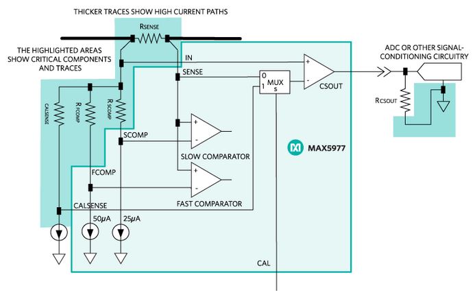 Figure 1. Applications diagram showing the critical components and traces for a MAX5977 circuit.
The circuit-breaker function compares the voltage across RSENSE to the voltages across RSCOMP and RFCOMP. See Figure 2. When the voltage across RSENSE exceeds the voltage across either RSCOMP or RFCOMP, the circuit breaker will trip. The voltages being compared will typically be in the 25mV to 100mV range. Improper component placement and layout can result in nuisance trips or failure to trip under some fault conditions.
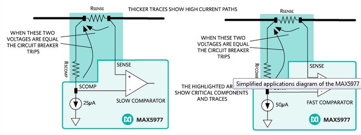
Figure 2. Simplified applications diagram of the MAX5977 fast and slow circuit-breaker functions.
The MAX5977’s current reporting senses the voltage across RSENSE through the IN and SENSE pins. See Figure 3. Internally, a transimpedance amplifier with a gain of 2500µS outputs a current on the CSOUT pin. An external resistor, RCSOUT, converts this current into a voltage and, along with RSENSE, sets the overall gain of the circuit. Similar to the circuit-breaker function, the voltage measured across RSENSE is quite small, typically ranging from a couple of millivolts to 50mV. Improper placement or routing of the components shown in Figure 3 results in reduced accuracy across RCSOUT.
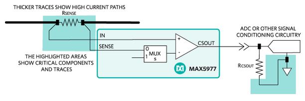 Figure 3. Simplified applications diagram for the MAX5977 current-reporting function.
The CALSENSE pin allows for a single-point calibration of the current reporting. See Figure 4. An external current source generates a known voltage across RCALSENSE. This calibration voltage is multiplexed into an external ADC through the CAL pin. The calibration voltage will typically be in the 25mV to 50mV range. Improper placement and routing will cause errors during calibration and adversely affect all future current measurements.
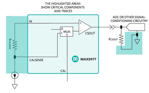 Figure 4. Simplified applications diagram showing the circuitry for single-point calibration of the current reporting.
Layout Guidelines
This section includes rough guidelines for proper placement and routing. These guidelines are not hard-and-fast rules, but provide a framework to help maximize the performance of the MAX5977. While proper placement and routing are always good ideas, circuits with higher RSENSE values are less susceptible to errors. As such, circuits with high RSENSE values can take some liberties without adversely affecting performance. Conversely, lower RSENSE values need to adhere more strictly to the suggested guidelines.
RSENSE Connections
Load current carrying traces that connect to RSENSE should be connected to the ends of RSENSE and not the sides. The width of these traces should be roughly the width of the pads at the connection point. See Figure 5. Proper connections of these traces prevent uneven current densities, and therefore, voltage differences across the pads.
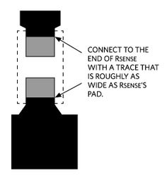 Figure 5. Connect the high-current traces to the ends of RSENSE and not the sides. Keep the trace widths roughly equal to the pad widths at the points of connection.
A four- (or six-) terminal sense resistor is recommended when using lower value resistances. If a two-terminal sense resistor is used, connect the voltage-sensing leads to RSENSE with a kelvin connection. See Figure 6.
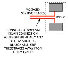 Figure 6. Diagram showing a kelvin connection on a two-terminal RSENSE.
Differentially route the voltage-sensing leads connected to RSENSE as long as possible and keep them as short as possible. Keep the voltage-sensing leads away from any noisy traces.
RCALSENSE, RSCOMP, and RFCOMP
RCALSENSE (if used), RSCOMP, and RFCOMP should be placed as close as possible to the MAX5977. Keep the traces from these resistors to the MAX5977 as short as possible.
The connection from RCALSENSE, RSCOMP, and RFCOMP to RSENSE should be made directly to the differentially routed kelvin-sensed traces. See Figure 7.
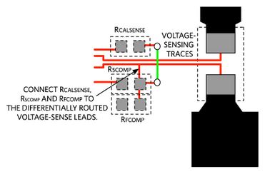 Figure 7. Connect RCALSENSE, RSCOMP, and RFCOMP to the differentially routed voltage-sense leads.
Keep RCALSENSE, RSCOMP, and RFCOMP, and their associated traces away from noisy traces.
RCSOUT
Less critical, but also important, is the placement and grounding of RCSOUT. RCSOUT is usually connected to an ADC or other signal-conditioning circuitry (we will use an ADC in this case). This ADC can be located a significant distance from the MAX5977 or, in some cases, can be located on a different board. Ground differences between the MAX5977 and the ADC can reduce measurement accuracy. Therefore, it is important to place and ground RCSOUT next to the ADC. See Figure 8.
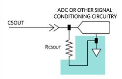 Figure 8. Ground RCSOUT directly at the ADC or signal-conditioning circuitry. This is especially important if the ADC or signal-conditioning circuitry is on a different board than the MAX5977.
Keep the CSOUT trace away from any noisy traces.
Grounding
The MAX5977 has two different grounds: AGND and GND. AGND (pin 3 and the exposed pad) is connected to the precision signals inside the MAX5977. The current sources connected to FCOMP and SCOMP are both grounded to AGND, along with other precision signals as shown in Figure 9. GND (pin 13) is used for the digital signals and the gate pulldown driver also shown in Figure 9.
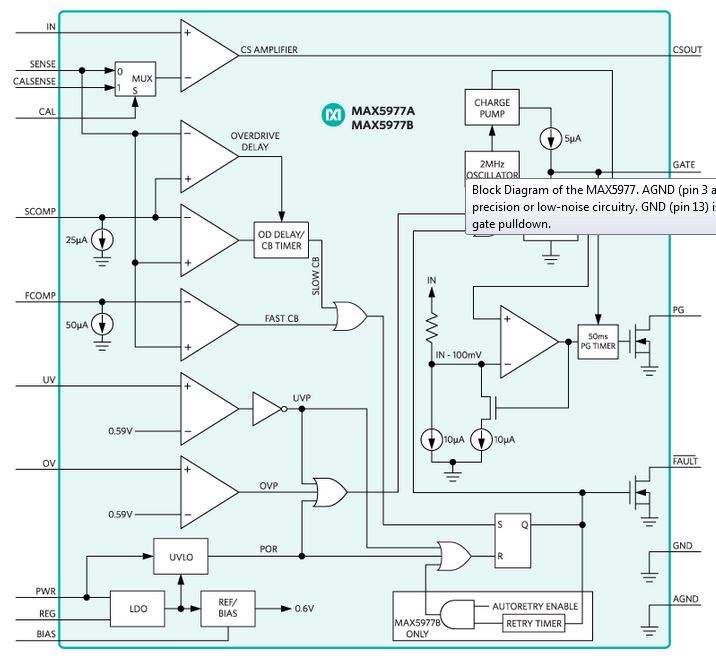 Figure 9. Block Diagram of the MAX5977. AGND (pin 3 and the exposed pad) is used for the precision or low-noise circuitry. GND (pin 13) is used for the digital circuitry and the gate pulldown.
Connect pin 3 and the exposed pad, both AGND, together through a short trace as shown in Figure 10. Connect the exposed pad to the ground plane with one or more vias. Note that the MAX5977’s power dissipation will be significantly less than 100mW. It is not necessary to have a large number of vias connected to the exposed pad for thermal reasons.
Connect GND (pin 13) directly to the ground plane with its own via as show in Figure 10.
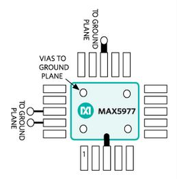
Figure 10. Connect pin 3 (AGND) directly to the exposed pad. Connect the exposed pad to the ground plane with a via or vias. Connect the GND pin (pin 13) to the ground plane with a via.
GATE and SOURCE
When an overcurrent event occurs, the MAX5977 turns off the external MOSFET by shorting the FET’s gate and source. In the case of a hard short, it is important to turn the external FET off as quickly as possible. Quickly turning off the FET prevents hard shorts from propagating to the bus. The MAX5977 has a very fast 200ns typical response time and a 500mA shorting current. The high shorting current is required to quickly discharge the external FET’s gate-to-source capacitance (CGS). Properly route the GATE and SOURCE to keep the FET turn-off time as short as possible.
The traces connecting the GATE and SOURCE pins to the external FET should be as short as reasonable to minimize parasitic inductance. Thicker traces should be used to also minimize inductance and to support the 500mA discharge current. See Figure 11.
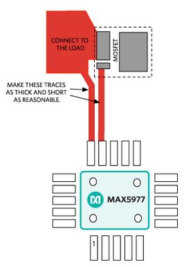
Figure 11. Connect the GATE and SOURCE pins to the external FET with short and wide traces. This keeps the turn-off time short by minimizing trace inductance.
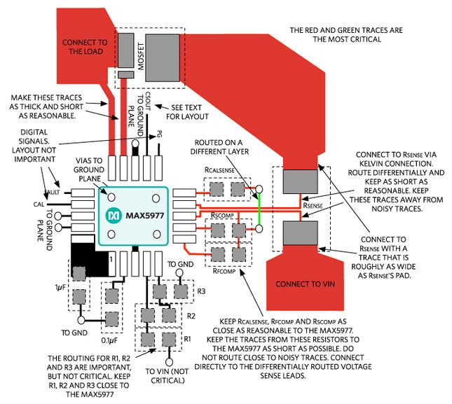
Figure 12 shows one possible layout with all of the above suggestions along with other guidelines.
Summary of placement and routing guidelines for the MAX5977 .
Figure 12. Summary of placement and routing guidelines for the MAX5977.
Effect of Poor Routing
Assume in Figure 13 that RSENSE is a 2010-sized 2.5mΩ resistor with 0.12in wide pad. Let’s also assume that the sensing points are incorrectly connected 0.12in away from the pads of the sense resistor.
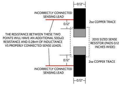
Figure 13. Improperly connecting to the sense resistor can lead to significant errors.
Each 0.12in × 0.12in trace between the sensing point and RSENSE will add roughly 250µΩ of resistance and 0.14nH of inductance (Note 1). Figure 14 shows the equivalent circuit.

Figure 14. Equivalent circuit of the improperly connected RSENSE shown in Figure 13.
The current reporting and slow-trip circuit breaker have filtering and should not be affected by the added inductance. However, the added resistance of 500µΩ will create a +20% error with respect to the 2.5mΩ sense resistor. For reference, the data-sheet current reporting error is ±4.1% worst case (Note 2). This small routing mistake has increased the overall error from roughly ±4% to +16%/+24%. A full 4x to 6x increase in error!
Both the added resistance and inductance impact the fast-trip comparator since it lacks filtering. A 10A/µs current transient through RSENSE will create an additional 2.8mV error on top of the 20% resistance error. Faster slew rates will create proportionally larger errors.
The errors introduced into the slow and fast circuit breaker thresholds can result in the MAX5977 turning off the downstream circuitry unnecessarily. Depending on the severity of these nuisance trips, the design could be rendered unusable.
Examples of Bad Placement and Routing
Figure 15 shows an example of bad placement and routing.
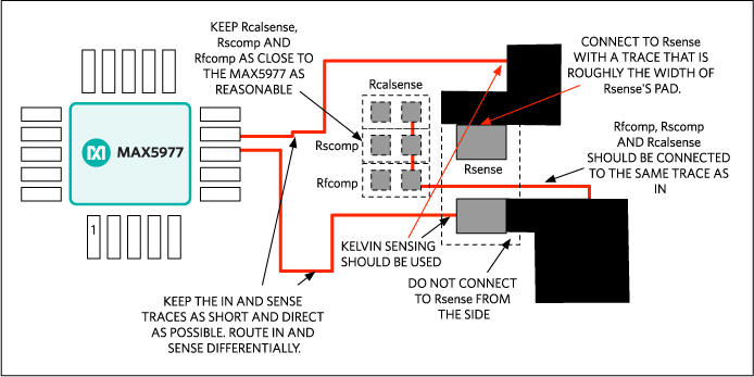
Figure 15. Example of incorrect placement and routing on a MAX5977 circuit.
Advertisement
Learn more about Maxim Integrated


