BY JUN LIU,
Principal Applications Engineer,
Intersil
www.intersil.com
Supercapacitors (SCs), also known as ultracapacitors and electric double-layer capacitors are finding use in a variety of power management applications. In automotive applications such as start-stop systems with regenerative braking, SCs can provide the energy needed to engage the starter to restart the combustion engine as well as accept the kinetic energy recovered during braking. SCs are advantageous because they can be charged and discharged significantly more times than traditional lead-acid batteries, and can also absorb energy more rapidly without degrading their expected lifetime. These capabilities also make SCs attractive for industrial backup power supply systems, quick-recharge cordless power tools and remote sensors where the frequent replacement of batteries isn’t practical.
This article addresses the challenges related to charging these large capacitors, and shows power system designers how to evaluate and select the best system configuration for backup energy storage. An SC charger solution is demonstrated, with waveforms and detailed interpretations presented.
System elaboration
There are many system configurations using SC banks as backup energy storage. To get started, designers will need to target their energy storage configuration and then decide at what voltage the energy can be stored. Selecting the solution depends on the power and voltage requirements of the load and the energy and voltage capabilities of the SC. Once the best solution is identified, tradeoffs between overall performances and cost must be made.
Figure 1 shows the block diagram of a high efficiency solution where the loads are devices requiring regulated input voltages (3.3, 5, 12 V, and others). The main supply of 48 V is supplying Switching Regulator 2 (SW2) in normal operation while simultaneously charging the SC bank to 25 V through Switching Regulator 1 (SW1). When the main supply is disconnected, the SC bank then supplies SW2 to maintain load operation without interruption.

Fig. 1: Block diagram of a battery backup system example using a supercapacitor bank
System design and challenges
Once an SC cell has been chosen, the system designer must select the target voltage at which each SC cell will be charged. This is done based on the rating curves of the SC. Most SC cells are rated in the range of 2.5 to 3.3 V at room temp—this rating falls at higher temps and with longer desired lifetime. Typically, the target voltage should be set below the maximum rated voltage to extend the operating life of the SC.
Next, the voltage desired for the bank of SCs and SW2 topology can be chosen. The SC bank configurations can be in parallel, series or a combination of series strings in parallel. Since the cell voltage rating is typically under 3.3 V and the loads often require equal or higher supplies, the options for cell configuration and SW2 will be to use a single cell with a boost converter or multiple cells in series and a buck or buck-boost regulator. To use a boost, we must ensure that as the SC discharges, the voltage doesn’t drop below the minimum operating input voltage for SW2. This can be up to half of the charged voltage of the SC, and for this reason, we’ll illustrate a bank that consists of a series combination of SCs and a simple buck regulator for SW1. Then, if energy requirements demand, multiple series strings will be placed in parallel.
If a series combination of SCs is chosen, the number of cells used must be selected based on the maximum desired voltage at the top of the string. More capacitors in series means higher voltage of the SC string with less capacitance. For instance, consider the choice of using two strings of four 2.7 V 10 F capacitors versus one string of eight (in series) of the same capacitor. While the same total charge and energy can be stored, the usable voltage range of the string makes the single series string advantageous. For example, to have a load requiring 5-V bias, the required voltage for SW2 is around 6 V, considering its maximum duty cycle and other dropout factors.
• The energy in a capacitor is W=CV2/2 and the energy that can be used is W= C/2(Vcharge2 – Vdischarge2)
• For two strings of four capacitors, the usable energy is W = 2*[(10 F/4)/2*((2.7 V*4)2-6 V2)] = 201.6 J
• The usable energy in the single string of eight (in series) is W = 1*[(10 F/8)/2*((2.7 V*8)2-6 V2)] = 269.1 J
Since both capacitor banks store the same total energy, the string with lower voltage has a greater percentage of charge wasted/unusable. In this case, the higher string voltage is preferable to fully utilize the SCs.
A third system challenge arises when considering how to charge the SC bank. Initially, when the SC voltage is 0, SW1 has to work at a condition similar to an output short for a fairly long period of time due to the high capacitance. A regular SW1 may get stuck in hiccup mode and fail to charge the SC. To protect the SC and SW1, additional current limiting function is necessary at the beginning of the charging stage. A good solution would be for SW1 to provide continuous charging current for an extended amount of time at almost no output voltage.
There are various methodologies to charge an SC. Constant current/constant voltage (CICV) is more commonly used and the preferred method as shown in Fig. 2 (CICV curve). At the beginning of the charge cycle, the charging device (SW1) operates in constant current mode providing a constant current to the SC such that its voltage is linearly increasing. The SC is charged to a target voltage, at which time the constant voltage loop becomes active and accurately controls the SC charge level to be constant to avoid over charging. Again, this preferred solution places requirements on the power management functions that will need to be considered.

Fig. 2: CICV supercapacitor charge control
Referring back to Fig. 1 as an example, with a main supply of 48 V, an SC bank voltage of 25 V and load voltages of 3.3, 5, 12 V, and more, a synchronous buck function for both SW1 and SW2 is appropriate. With the primary challenge relating to SC charging, the choice for SW1 is critical. The ideal solution for SW1 would require power management functionality that is capable of operating with high input (48 V) and output (25 V) voltages while also providing CICV regulating capability.
Demonstration of a supercapacitor charger solution
To demonstrate the SC charging behavior, we’ll use a sync buck regulator example. We’ll show the key problems and resolving techniques, and use experimental waveforms to aid our understanding.

Fig. 3: Simplified schematic of a sync buck regulator achieving CICV SC charging control
Figure 3 shows the simplified schematic of Intersil’s ISL78268 controlling a synchronous buck regulator that achieves CICV control. To charge a supercapacitor bank to 25 V with CICV control, the following capabilities were considered when selecting the controller:
1. Synchronous buck controller that can operate with VIN >= 48 V and VOUT >= 25 V.
2. Constant current and constant voltage regulating capability with automatic transitions between regulation modes.
3. Accurate current sense inputs for the CI portion that operate over the supply voltages of the system. Referring to Fig. 3, the controller is sensing the inductor’s continuous current, which is the charging current. The controller’s current sense amplifier must withstand the common mode voltage, which is 25V in this case.
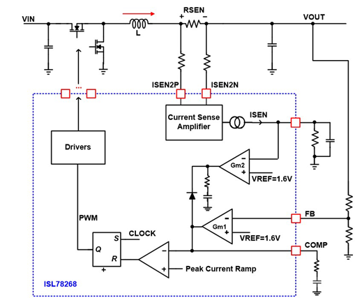
Figure 4 shows a small section of the ISL78268 synchronous buck controller’s functional block diagram. As shown, there are two independent error amplifiers labeled Gm1 and Gm2, which serve to regulate constant voltage (Gm1) and constant current (Gm2).
Error amplifier Gm1 works for CV close loop control. It compares the feedback voltage at FB to the internal 1.6-V reference voltage and creates an error voltage at the COMP pin. The FB pin is tied to a resistor divider from the output voltage and is set such that FB will be 1.6 V when the output is at the desired voltage. The COMP voltage then represents the difference between the desired output voltage and the actual output voltage. COMP is then compared to the peak inductor ramp to generate the PWM signal to control the output voltage to be constant.
Error amplifier Gm2 works for CI close loop control. It compares IMON/DE pin voltage and the internal 1.6-V reference and creates an error output at the COMP pin. The IMON/DE pin voltage is generated internally and represents the average output inductor load current. Thus, the COMP voltage when Gm2 loop is active (the diode between the output of Gm1 and Gm2 effectively selects which loop is active), represents the difference between the desired output current and the actual output current. COMP is then compared to peak inductor ramp to generate PWM signal to control the output current to be constant.
At the beginning of the charge stage before the SC voltage reaches its target, Gm2 is dominantly driving the COMP pin, causing the PWM output to achieve CI control. When the SC voltage is charged to target, the charging current is reduced causing IMON/DE pin voltage to fall low and CI loop disengages (when IMON/DE
The ISL78268 buck controller has both peak current mode control for PWM generation (reliable cycle-by-cycle peak current modulator) and outer constant average current loop ideal for SC charging.

Fig. 4: ISL78268 CICV loop simplified block diagram
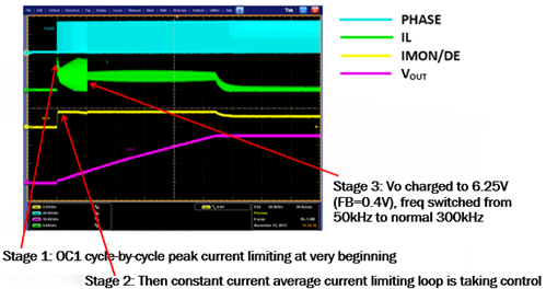
Now we’ll highlight the realized SC charging implementation. Figures 5, 6 and 7 show the experimental waveforms of the synchronous buck controlled by the ISL78268 to charge a SC bank (12 50 F/2.7 V SC in series). The SC will be charged to 25 V from the main supply.

Fig. 5: Bench waveforms of SC charging
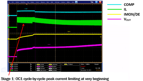
Figure 5 shows there are several stages for the SC charging. Initially, at stage 1, Vo is barely 0. The average current signal on the ISL78268’s IMON/DE pin has not yet reached 1.6 V (the reference value for the desired charging current), so the CI loop has not yet engaged. At this stage, the inductor’s peak current is cycle-by-cycle limited to fixed OC threshold. At the beginning of the charging state when the VOUT is low (FB
Figure 6 shows a zoomed in waveform of stage 1. Stage 2 starts when the IMON/DE pin voltage (yellow trace) reaches 1.6 V. Here, the CI loop engages and pulls the COMP signal (cyan trace) lower, thus beginning to regulate the output current and causing the IMON/DE pin voltage to remain constant. IMON/DE pin voltage represents the sensed average output current signal. The IL waveform (green trace) shows the average current is controlled to be constant during stage 2. The output voltage (pink trace) shows the SC is linearly charged by the constant charging current.

Fig. 6: Zoom in bench waveforms of SC charging at Stage 1
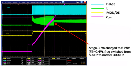
Stage 3 starts when the FB pin detects 0.4V (Fig. 7). After detection, the constant current regulation is known to be fully engaged, so the switching frequency can be automatically adjusted to the programmed frequency of 300 kHz. With higher switching frequency, the inductor current ripple (green trace) is significantly reduced. The output voltage (pink trace) continues to linearly increase, indicating the SC is being linearly charged.

Fig. 7: Bench waveforms of SC charging
Referring back to Fig. 5, stage 3 proceeds until Vo reaches the target voltage of 25 V. Once that occurs, the CV loop engages and regulates the output voltage. The average current loop disengages. Fig. 5 shows that the output voltage (pink trace) levels off and the inductor current drops low. The IMON/DE pin, representing the average charging current also falls, signifying the end to constant current regulation.
Supercapacitors are adopted as energy storage solutions in certain automotive, industrial and consumer products due to their intrinsic physical characteristics that provide advantages over traditional batteries. To maximize the energy stored in the SC bank, it’s often best to stack several SC cells in series to realize high bank voltages. When charging, it is preferable to use a CICV charging methodology to limit the high currents that would otherwise flow due to the low ESR of the SC if charging to a constant voltage. The constant current makes charging losses controllable within the SC, which can reduce heat generation and extend the life of the SC. Thus, it is advantageous for the charging circuits to tolerate high voltages and provide CICV regulation capability.
Advertisement
Learn more about Intersil


